The welding process of the BGA (Ball Grid Array) chip in PCB assembly is a complex and precise process involving several key steps and details. The following is a detailed analysis of the BGA chip welding process:
First, preparation before welding
PCB preparation
Clean: Use alcohol or special detergent to clean the surface of the PCB board, remove oil and dust, and ensure that the welding pad is free of dust, grease or other pollutants.
Flux or solder paste coating: Apply an appropriate amount of flux to the corresponding solder pad position of the PCB or print a uniform layer of solder paste through the steel screen in advance. Flux helps to improve solder flow and solder quality, and solder paste is used to form solder connections.
Spot adhesive: Pre-spot an appropriate amount of adhesive on the BGA pad position on the PCB board to fix the BGA chip and prevent it from moving during welding.
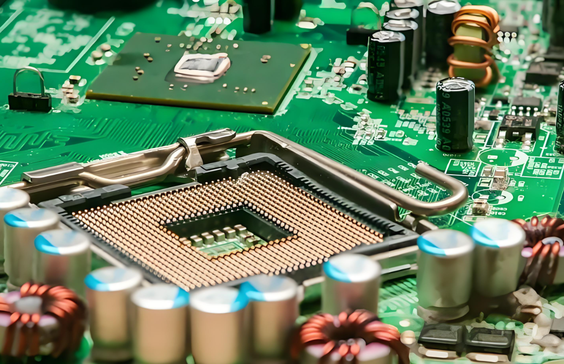
BGA chip ready
Check: Ensure that the BGA chip has no damage and the welding ball is complete. The quality of the welding ball directly affects the welding effect, so it must be carefully checked.
Positioning: According to the mark on the PCB, determine the correct placement position and direction of the BGA chip.
Equipment and material preparation
Welding equipment: including reflow furnace, heat gun, microscope, solder paste printing machine, cleaning fluid, X-ray testing equipment, etc.
Welding materials: solder paste (usually tin-silver-copper alloy), flux (no-wash flux can reduce subsequent cleaning work), adhesive, etc.
Second, the welding process
Chip placement
Alignment: The BGA chip is placed in a preset position on the PCB using a high-precision mounter or manually, and an optical or laser alignment system ensures that the chip is precisely aligned with the pad, usually within a tolerance of ±0.05mm.
Fixed: The mounted PCB board is placed in the oven and cured according to the curing temperature and time of the adhesive to ensure that the chip will not move during the welding process.
Solder paste printing
Select solder paste: Select the appropriate solder paste according to the size of the solder ball of the BGA chip and the requirements of the PCB board.
Printing: Use the solder paste press to accurately print the solder paste on the BGA pad to ensure that the solder paste is evenly distributed without missing or accumulation.
Preheating and welding
Preheat: Put the PCB into the reflow furnace and preheat according to the set temperature curve. The preheating temperature and time are determined according to the thickness of the PCB board and the type of solder paste to activate the flux and evaporate the solvent in the solder paste.
Welding: After preheating, enter the reflow welding stage. The temperature gradually increases to a peak (usually around 260°C), allowing the solder paste to melt and form a good solder joint with the PCB pad. During the welding process, the temperature curve needs to be strictly controlled to ensure the welding quality.
Cooling: After welding is completed, let the PCB board cool naturally. It is necessary to control the cooling speed during the cooling process to avoid welding defects such as holes and cracks.
Third, welding post-processing and testing
cleanse
Remove residue: Clean the welded PCB board with a cleaning solution to remove residual flux and welding slag. The cleaning step is particularly important in cases where non-wash-free flux is used.
Quality inspection
Appearance inspection: Use a microscope to check the welding quality and ensure that the welding between the ball and the pad is good, and there are no defects such as virtual welding, bridge or cold welding.
X-ray inspection: Complete internal inspection of BGA solder joints using X-ray inspection equipment. X-ray inspection can see through the inside of the solder joint, detect holes, cracks and other defects, to ensure the integrity and reliability of the welding.
Electrical test: Perform electrical test to ensure that the connection between BGA chip and PCB board is normal and the function meets the requirements.
Fourth, welding process precautions
Temperature curve setting
Reasonable adjustment: Temperature curve has an important effect on welding quality. Parameters such as preheating temperature, maximum temperature and holding time need to be flexibly adjusted according to factors such as solder paste type and PCB size.
Avoid overheating: Excessive welding temperature may cause damage to the BGA chip or PCB board, so the temperature must be strictly controlled.
Alignment accuracy
High-precision equipment: Use high-precision mounters and alignment systems to ensure precise alignment of the chip and pad.
Infrared scanning imaging: can assist alignment, improve alignment accuracy.
Welding environment
Clean and dust-free: BGA welding needs to be carried out in a clean, dust-free and constant temperature environment to prevent pollutants such as dust from affecting the quality of welding.
Esd prevention: Take ESD preventive measures to prevent damage to BGA chips caused by static electricity.
Welding defect prevention
Avoid bridge: control the printing quality of solder paste and welding process parameters to prevent the formation of bridge between adjacent solder joints.
Prevent virtual welding: ensure that the welding temperature and time are sufficient, so that the solder paste is fully melted and forms a good welding joint with the pad.
Fifth, welding process improvement and optimization
Introduce new technology
Laser alignment system: improve alignment accuracy and efficiency.
Intelligent temperature control system: precisely control the temperature curve in the welding process, improve the welding quality.
Process parameter optimization
Experiment and test: Through experiment and test, find the best combination of welding process parameters, improve welding quality and production efficiency.
Continuous improvement: Continuous improvement and optimization of the welding process based on feedback and test results in the production process.


