Application and Advantages of AOI Inspection Technology in PCBA Manufacturing
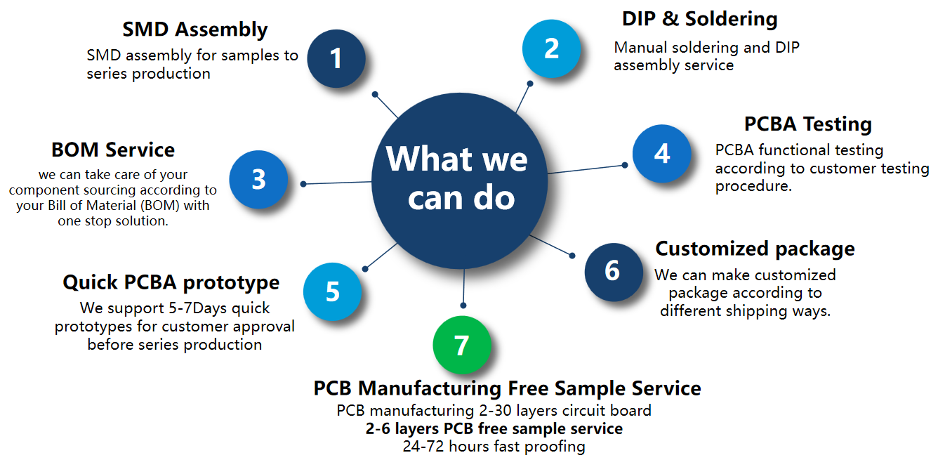
In today's highly automated and electronic era, the manufacturing process of printed circuit board assembly (PCBA) has increasingly higher requirements for precision and efficiency. As a key link in PCBA manufacturing, automated optical inspection (AOI, Automated Optical Inspection) technology is playing an increasingly important role. XDCPCBA, as a professional supplier with 2-30-layer PCB production capacity, not only demonstrated its strong production strength, but also deeply demonstrated its deep understanding of customer needs by launching 2-6-layer PCB free sample service. This article will deeply explore the principles of AOI inspection technology and its application in PCBA manufacturing, and introduce the unique advantages of XDCPCBA as a professional PCB and PCBA manufacturer at the end of the article.
1. Basic principles of AOI inspection technology
AOI inspection technology is an automated inspection method based on image processing. Its core is to use high-resolution cameras to capture images of objects to be inspected, and analyze and compare these images through advanced image processing algorithms to identify defects in the manufacturing process. This process can be roughly divided into the following steps:
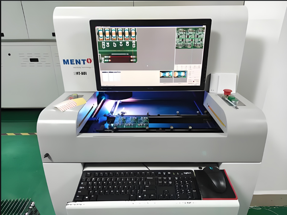
Image acquisition: The AOI system uses a high-resolution camera to shoot the PCB or PCBA to be inspected to obtain high-quality image data. These image data contain detailed information such as all components, solder joints, and circuits on the circuit board.
Image preprocessing: The acquired images often contain noise, uneven lighting, etc., so preprocessing is required. The preprocessing steps include denoising, contrast enhancement, color correction, etc. to ensure the accuracy of subsequent analysis.
Feature extraction: In the preprocessed image, the AOI system will identify and extract key features, such as the shape, size, position of the component, and the shape of the solder joint. These features are an important basis for judging product quality.
Defect detection: The extracted features are compared with the preset standards or templates. The AOI system can automatically identify areas that do not meet the requirements, such as missing components, misalignment, poor welding, and other defects.
Result output and feedback: The AOI system presents the test results to the user in an intuitive way, such as highlighting the defect location and generating a test report. At the same time, these test results can also be used as feedback in the production process to guide the improvement of subsequent processes.
2. Application of AOI detection technology in PCBA manufacturing
In the PCBA manufacturing process, the application of AOI detection technology is mainly reflected in the following aspects:
Post-component mounting inspection: In the SMT (surface mount technology) process, the AOI system can quickly inspect the components after mounting to ensure that the position, direction, quantity, etc. of the components meet the design requirements. This helps to promptly discover and correct errors in the mounting process and avoid waste in subsequent processes.
Welding quality inspection: Welding is one of the key links in PCBA manufacturing. The AOI system can carefully inspect the solder joints after welding and identify welding defects such as cold soldering, continuous soldering, and leaking soldering. This helps to ensure welding quality and improve product reliability and stability.
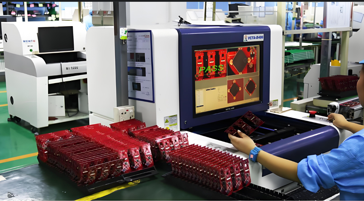
Finished product final inspection: In the final stage of PCBA manufacturing, the AOI system can perform a comprehensive final inspection of the finished product. This includes inspections of the appearance of the circuit board, the integrity of the components, the connectivity of the lines, and many other aspects. Final inspection helps ensure that the quality of the final product meets customer requirements and improves customer satisfaction.
3. Advantages and Challenges of AOI Inspection Technology
AOI inspection technology has significant advantages in PCBA manufacturing, such as fast inspection speed, high accuracy, and non-contact inspection. However, the application of AOI technology also faces some challenges, such as the complexity of image processing algorithms, the diversity of defect types, and false positives and false negatives during the inspection process. In order to solve these challenges, researchers are constantly developing more advanced image processing algorithms and inspection technologies to improve the performance and reliability of AOI systems.
4. XDCPCBA's Professional Strength and Advantages
As a PCB and PCBA manufacturer with rich experience and advanced technology, XDCPCBA has demonstrated unique advantages in the application of AOI inspection technology.
Strong production capacity: XDCPCBA has the production capacity of 2-30 layers of PCB, which can meet the diverse needs of different customers. Its advanced production equipment and process flow ensure the high quality and high efficiency of PCB production.
Professional AOI inspection system: XDCPCBA is equipped with advanced AOI inspection systems that can perform comprehensive automated inspection of PCBA. These systems use the latest image processing algorithms and inspection technologies to accurately identify various defects and ensure the reliability and stability of products.
Free sample service: In order to help customers better understand XDCPCBA's production capacity and product quality, the company has launched a 2-6 layer PCB free sample service. Customers can get high-quality PCB samples through this service, so that they can trust XDCPCBA's products and services more.
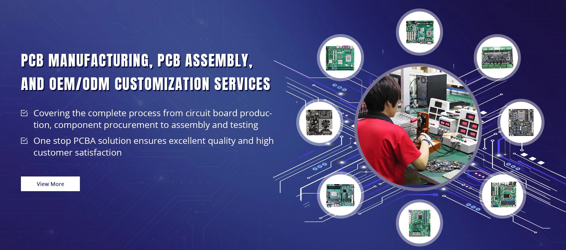
Comprehensive PCBA processing services: In addition to PCB production, XDCPCBA also provides comprehensive PCBA processing services. From component procurement, mounting, welding to testing, assembly and other links, XDCPCBA can provide professional technical support and services to ensure that customers' products can be produced on time, in quality and in quantity.
Deep customer understanding: XDCPCBA is well aware of the importance of customer needs. Therefore, the company always puts customer needs first and is committed to providing customers with the best products and services. Whether it is product design, production process or after-sales service, XDCPCBA can customize and optimize according to the actual needs of customers.
Conclusion
With the continuous development of the electronics industry, PCBA manufacturing will have higher and higher requirements for precision and efficiency. As a key link in PCBA manufacturing, AOI detection technology is playing an increasingly important role. As a PCB and PCBA manufacturer with strong production capacity and professional AOI inspection system, XDCPCBA will continue to be committed to providing customers with the best products and services. Through continuous innovation and improvement, XDCPCBA will provide customers with more efficient, reliable and flexible PCBA manufacturing solutions, and jointly promote the development and progress of the electronics industry. In the future, XDCPCBA will continue to uphold the "customer-centric" concept, continuously improve its technical strength and service level, and create greater value for customers.


