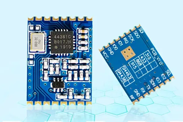
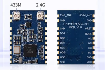
A UWB (Ultra Wideband) positioning technology has demonstrated unique application value in multiple fields due to its centimeter level accuracy, low latency, and strong anti-interference capabilities. The following are its core application scenarios and specific cases:
1、 Consumer Electronics and Smart Life
1. Interaction between smartphones and IoT devices
Scenario: The mobile phone accurately perceives the location of surrounding devices through UWB, achieving contactless interaction.
Case: The Apple iPhone 11/12 series is equipped with the U1 chip, which supports the "space sensing" function and can be used to control the volume of HomePod speakers and quickly find AirTag trackers (with centimeter level accuracy).
Extension: In smart homes, when the phone is close to the smart door lock, it automatically unlocks or points to the TV to switch channels.
2. Smart wearables and personnel tracking
Scenario: Preventing children/elderly from getting lost, tracking pets, and monitoring sports and health.
Case: Huawei Watch GT 4 supports UWB tag linkage, allowing parents to view their child's precise location in the mall in real-time; The gym tracks the user's movement trajectory and analyzes their posture through UWB.
2、 Industrial and Intelligent Manufacturing
1. Factory assets and personnel positioning
Scenario: Tracking production line equipment, AGV carts, worker positions, optimizing production processes, and ensuring safety.
Case: In automobile manufacturing factories, UWB positioning systems monitor the positions of robotic arms and material trucks in real time to avoid collisions; High risk areas (such as chemical workshops) restrict personnel from entering and trigger alarms.
Advantages: Strong resistance to metal obstruction and multi-path interference, suitable for complex industrial environments.
2. Warehouse logistics and automated sorting
Scenario: Accurately locate shelves, pallets, and AGV carts in an intelligent warehouse to improve sorting efficiency.
Case: JD's "Asia No.1" warehouse adopts UWB technology, and AGV cars automatically park on shelves through centimeter level positioning, cooperating with robotic arms to complete cargo grabbing, improving sorting efficiency by more than 30%.
3、 Indoor Navigation and Smart Space
1. Navigation for large venues (shopping malls, airports, hospitals)
Scenario: Provide real-time indoor map navigation for users, accurately guiding them to stores, boarding gates, consultation rooms, etc.
Case: Shanghai Pudong Airport introduces UWB positioning system, allowing passengers to view real-time location through a mobile app and navigate to security or boarding gates, reducing the average time by 50%; The museum achieves "precise guidance" through UWB, automatically playing explanations when approaching exhibits.
2. Assistance for blind and visually impaired individuals
Scenario: Real time path guidance is provided to visually impaired individuals through the linkage of UWB tags and obstacle sensors.
Case: Microsoft collaborates with a non-profit organization to develop the "Soundscape" system, which combines UWB positioning and audio feedback to help blind people identify obstacles and plan safe routes.
4、 Intelligent Transportation and Connected Vehicles
1. Keyless entry and vehicle safety
Scenario: When the car owner approaches the vehicle, UWB accurately identifies their identity and automatically unlocks the doors (to prevent relay attacks).
Case: BMW Digital Key Plus uses UWB technology to determine whether the owner is actually approaching the vehicle (rather than signal relay forgery), avoiding key duplication and theft.
2. Vehicle to vehicle/infrastructure collaboration (V2X)
Scenario: The vehicle perceives the real-time position of surrounding vehicles through UWB, predicts collision risks, and assists in autonomous driving.
Case: Ford tests UWB technology for automatic parking in parking lots, where vehicles achieve centimeter level precision parking by locating surrounding obstacles and parking lines; On highways, UWB can improve the accuracy of distance monitoring and reduce rear end collisions.
5、 Special Scenarios and Industry Applications
1. Tunnels and underground engineering
Scenario: Positioning workers and equipment during subway construction and mining to ensure emergency rescue efficiency.
Case: A tunnel project in Switzerland uses UWB positioning system to monitor the position of construction personnel in real time. Once a collapse occurs, the system can quickly lock in the coordinates of trapped personnel, shortening the rescue time.
2. Autonomous indoor flight of unmanned aerial vehicles
Scenario: In indoor inspection and logistics distribution, drones use UWB to achieve centimeter level positioning and avoid obstacles.
Case: Amazon Prime Air tests UWB for indoor drone delivery, accurately landing on designated desktops; The power company uses UWB positioning drones to autonomously inspect equipment in the substation.
6、 Medical and Health Management
1. Hospital assets and patient tracking
Scenario: Track wheelchairs, infusion pumps, and high-risk patients (such as Alzheimer's disease patients) to prevent them from getting lost or losing equipment.
Case: The Mayo Clinic in the United States has deployed a UWB system, allowing nurses to view the location of oxygen cylinders in real-time through a tablet, reducing device search time; In the psychiatric ward, patients wear UWB tags that automatically sound an alarm when they cross the line.
2. Precise surgical positioning
Scenario: Combining UWB with medical imaging to assist doctors in accurately locating lesions or instrument positions during surgery.
Research direction: Some medical institutions are exploring the use of UWB for minimally invasive interventional surgery, reducing radiation exposure and surgical errors by locating the position of the catheter.
Summary: The Core Advantages and Future Trends of UWB
Advantages: Compared to technologies such as Bluetooth and WiFi, UWB has irreplaceable advantages in precision (centimeter level vs. meter level), anti-interference (wideband low-power), and real-time (nanosecond level pulse).
Trend: With the decrease in chip costs (driven by manufacturers such as Decawave and Apple) and standardization (IEEE 802.15.4z), UWB will penetrate from high-end scenarios (such as automotive and industrial) to the consumer market, becoming one of the underlying positioning technologies for the "Internet of Things".
If you need to further understand the technical details or implementation plan of a certain scenario, feel free to ask additional questions at any time!


