In PCB (Printed Circuit Board) layout, the reasonable arrangement of components is a key step to improve manufacturability. The following are some layout strategies and suggestions aimed at optimizing the component layout and thereby enhancing the manufacturability of the PCB:
First, follow the design principle of manufacturability
Consider the PCB manufacturing process:
When making the layout, it is necessary to understand and consider the process capabilities and limitations of the PCB manufacturer, such as the minimum line width, minimum spacing, and hole size, etc.
Avoid designing boards that cannot be manufactured and ensure that the layout complies with the manufacturer's process requirements.
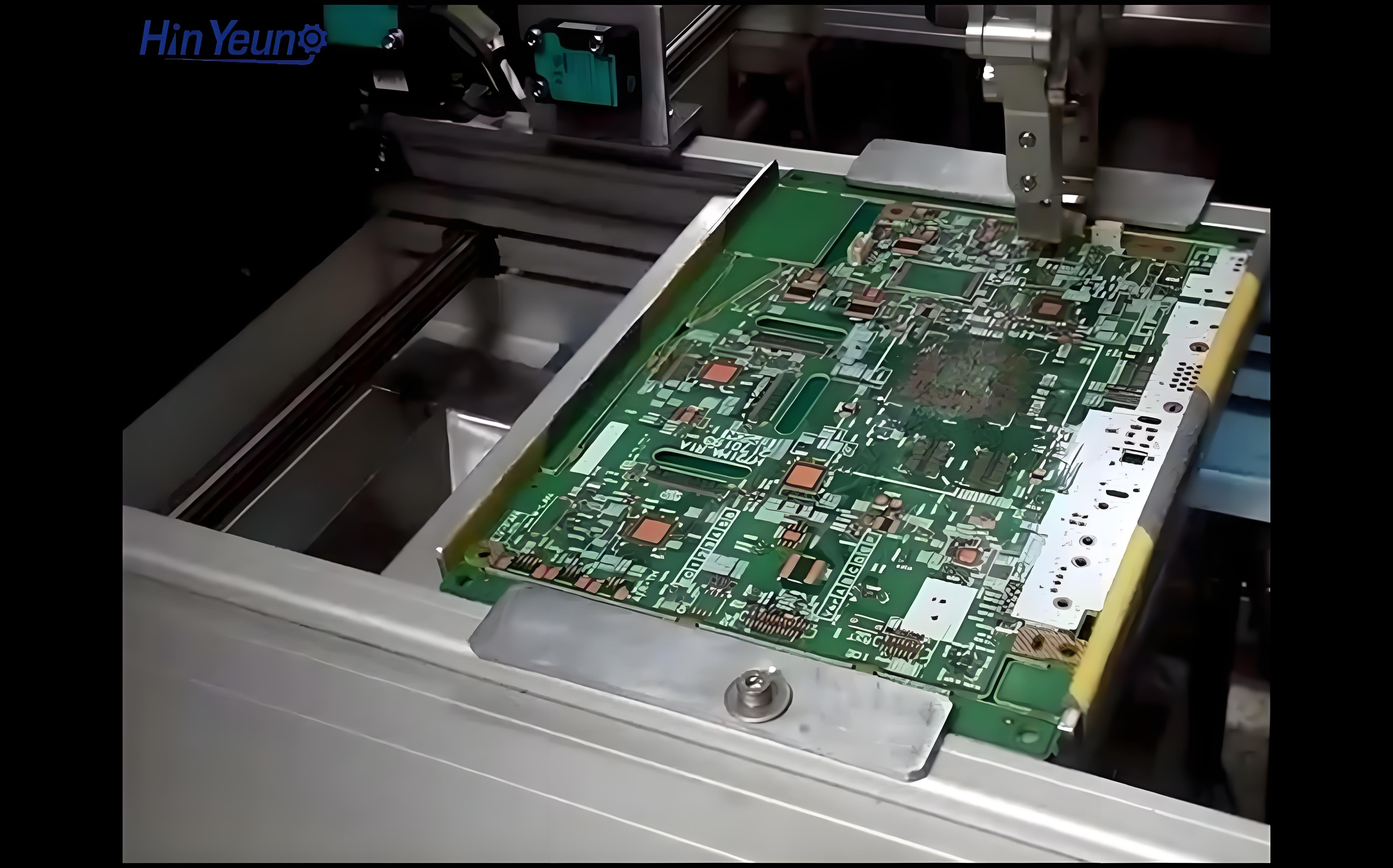
Convenient for automated production
The layout should facilitate the automated production processes such as surface mount technology (SMT), through-hole technology (through-hole), and soldering.
Reserve sufficient operating space for the robotic arm to prevent the component spacing from being too small or the layout from being overly crowded, which may cause the chip placement heads to collide or fail to mount accurately.
Second, optimize the layout of components
Zoning by function:
Concentrate the components related to the functions for easy wiring and debugging.
For example, the power module is surrounded by filter capacitors, inductors, etc., forming a stable power supply unit; The signal processing chip is adjacent to the corresponding amplification and filtering circuits, shortening the signal transmission path.
Unify the component direction:
Align similar components in the same orientation to facilitate efficient and error-free soldering.
The directions of polar devices should not exceed two. It is best to unify the directions to reduce assembly errors.
Avoid layout conflicts:
Avoid placing large components after small ones to prevent small components from having mounting issues due to the influence of large component soldering.
Sufficient space for insertion and soldering should be left around the plug-in components. The diameter of the insertion holes should be slightly larger than the diameter of the component pins.
Pay attention to the heat dissipation issue:
High-temperature components should be placed in well-ventilated locations and kept at a certain distance from other components to facilitate heat dissipation.
For components that require heat dissipation, heat dissipation measures such as heat sinks or heat pipes can be considered.
Consider testing and maintenance:
When laying out, sufficient space should be reserved for testing and maintenance.
Test points are set at key signal nodes and power supply nodes to facilitate measurement using test instruments.
Third, specific layout techniques
Edge component layout
Prioritize the placement of edge components such as connectors, switches, and jacks, as these components are usually immobile due to mechanical housings.
Avoid placing sensitive high-speed devices near the edge of the circuit board to reduce the impact of electromagnetic interference (EMI).
Layout of high-frequency components
High-frequency components should be placed as close as possible to shorten the length of high-frequency signal lines and reduce signal interference.
For high-frequency components that require shielding, measures such as using shielding covers or grounding copper sheets can be considered.
Power supply and grounding layout:
Placing the power supply and ground plane layers inside the circuit board and keeping them symmetrical and centered helps prevent the circuit board from deforming.
When powering the IC, a common channel should be used to supply power to each power source to ensure that the wiring is stable and of moderate width.
Avoid layout overlap and intersection:
Components should avoid overlapping and cross-wiring to prevent short circuits and signal interference.
For unavoidable cross-wiring, a vertical cross-wiring method should be adopted and the line spacing should be increased to reduce interference.
Consider the warpage and deformation of the PCB:
Uneven PCBS can lead to inaccurate positioning, affecting component insertion and automatic plug-in installation.
Therefore, when laying out, it is advisable to avoid placing too many heavyweight components on one side of the PCB as much as possible to reduce warping and deformation of the PCB.
Set auxiliary edges and positioning holes:
Top clamping edges of 3 to 5 millimeters should be set on both the upper and lower sides of the PCB to facilitate the transmission and positioning of automated equipment.
Installation positioning holes are usually pre-designed on the board. The positioning holes should be in a no-hole state (unmetallized and non-conductive), and the hole diameter and position should be determined according to the external environment of the PCB installation.
Fourth, inspection and optimization after layout
Use the Design Rule Check (DRC) tool:
After the layout is completed, use the DRC tool to conduct a comprehensive inspection of the PCB layout to ensure that it complies with the design rules and standards.
According to the inspection results of the DRC tool, the layout is optimized and adjusted.
Conduct signal integrity analysis:
Conduct signal integrity analysis on high-speed signal lines to ensure the integrity and accuracy of signal transmission.
Based on the analysis results, adjust parameters such as the length of the signal line and impedance matching to reduce signal reflection and interference.
Communicate and collaborate with the manufacturer:
After the layout is completed, communicate and collaborate with the PCB manufacturer to ensure that the layout meets the manufacturer's process requirements.
Based on the feedback and suggestions from the manufacturer, the layout is optimized and adjusted to enhance manufacturability.
By following the above layout strategies and suggestions, the manufacturability of PCBS can be significantly enhanced, problems and costs during the production process can be reduced, and product quality and production efficiency can be improved.


