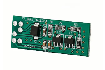
In the developing process of PCB manufacturing, common problems and their solutions are as follows. The occurrence of these problems may directly affect the accuracy, resolution of the circuit pattern and the electrical performance of the final product:
First, incomplete development (residual lines)
Problem manifestation: After development, there is still a dry film on the PCB surface that has not been removed, resulting in incomplete circuit patterns or the risk of short circuits.
Possible reasons:
Insufficient developer concentration: The activity of the developer decreases and it cannot completely dissolve the unexposed dry film.
Too short development time: Insufficient development time results in the dry film not being completely removed.
The developer temperature is too low: A temperature that is too low affects the development reaction rate.
Overexposure of dry film: Overexposure leads to excessive polymerization of the dry film, making it difficult to develop.
Solution:
Regularly test the concentration of the developer solution: Use a concentration meter to measure the concentration of the developer solution, and replenish the developer solution in time or replace it with new solution.
Optimize the development time: Adjust the development time according to the type of dry film and the thickness of the PCB to ensure that the dry film is completely removed.
Control the temperature of the developer: Keep the temperature of the developer between 25 and 30°C to enhance the development efficiency.
Adjust the exposure parameters: Reduce the exposure time or lower the exposure energy to avoid overexposure of the dry film.
Second, overdevelopment (line etching)
Problem manifestation: During the development process, the edges of the exposed dry film are dissolved, causing the line pattern to become thinner or open circuits to occur.
Possible reasons:
Excessive developer concentration: The developer is too active, causing the edges of the exposed dry film to dissolve.
Excessive development time: An overly long development time leads to excessive dissolution of the dry film.
Excessively high developer temperature: A temperature that is too high accelerates the developing reaction, causing excessive dissolution of the dry film.
Solution:
Adjust the concentration of the developer: Reduce the concentration of the developer to decrease its activity.
Shorten the development time: Adjust the development time according to the dry film type and PCB thickness to avoid over-development.
Control the temperature of the developer: Keep the temperature of the developer within a reasonable range to avoid it being too high.
Third, uneven development
Problem manifestation: The development effects of different areas on the PCB surface are inconsistent, resulting in a decrease in the accuracy of the circuit graphics.
Possible reasons:
Uneven developer spray: Malfunction of the developer spray system or nozzle blockage leads to uneven distribution of the developer.
Unstable PCB transmission speed: The PCB transmission speed in the developer is unstable, resulting in inconsistent development times.
Poor developer circulation: A malfunction in the developer circulation system leads to uneven concentration and temperature of the developer.
Solution:
Inspect the developer spray system: Regularly clean the nozzles to ensure even spraying of the developer.
Optimize PCB transfer speed: Adjust the PCB transfer speed to ensure consistent development time.
Improve the developer circulation: Inspect the developer circulation system to ensure uniform developer concentration and temperature.
Fourth, dry film residue after development
Problem manifestation: After development, there is still dry film residue on the PCB surface, which affects the subsequent etching process.
Possible reasons:
Poor adhesion of dry film: Insufficient adhesion between the dry film and the copper surface leads to incomplete detachment of the dry film during the development process.
Underexposure: Insufficient exposure energy leads to incomplete polymerization of the dry film, making it prone to residue during development.
Improper selection of developer: The developer does not match the dry film, resulting in poor developing effect.
Solution:
Enhance dry film adhesion: Optimize the pretreatment process to ensure the copper surface is clean and free from contamination, thereby improving the adhesion of the dry film.
Adjust the exposure parameters: Increase the exposure time or raise the exposure energy to ensure that the dry film is fully polymerized.
Select the appropriate developer: Choose the matching developer based on the dry film type to ensure the developing effect.
Fifth, the edges of the lines are rough after development
Problem manifestation: After development, the edges of the lines are not smooth, with burrs or serrations appearing, which affects the accuracy of the lines.
Possible reasons:
Excessive developer activity: The developer activity is too strong, causing the edges of the circuit to be overly dissolved.
Excessive development time: The development time is too long, causing the edges of the lines to be corroded.
Poor dry film quality: Unstable dry film quality leads to rough edges of the lines after development.
Solution:
Adjust the activity of the developer: Reduce the concentration or temperature of the developer to decrease its activity.
Shorten the development time: Adjust the development time according to the dry film type and PCB thickness to avoid over-development.
Select high-quality dry film: Use dry film of stable quality to ensure smooth edges of the lines after development.
Sixth, PCB surface contamination after development
Problem manifestation: Stains or residues appear on the PCB surface after development, affecting subsequent processes.
Possible reasons:
Developer contamination: Impurities or contaminants mixed into the developer can cause contamination of the PCB surface.
Incomplete water washing: Insufficient water washing after development leads to the residue of the developing solution.
Improper cleaning of the developer: The interior of the developer was not thoroughly cleaned, resulting in contamination of the PCB surface.
Solution:
Regularly change the developer solution: Regularly change the developer solution to prevent contamination of the developer solution.
Optimize the water washing process: Increase the frequency of water washing or extend the water washing time to ensure that the developer residue is completely removed.
Strengthen the cleaning of the developer: Regularly clean the interior of the developer to ensure the PCB surface is clean.


