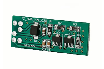
Automatic Optical Inspection (AOI) plays a crucial role in PCB manufacturing, running through multiple stages of PCB manufacturing, from the production of inner layer patterns to the final assembly inspection, undertaking key quality control tasks. The following is a detailed introduction to its applications, advantages, and limitations:
Application scenarios
Inner layer pattern detection: In the inner layer manufacturing of PCBS, the etching process may cause problems such as short circuits, open circuits or pattern offsets. The AOI system can quickly detect etching defects such as short circuits, open circuits, pattern breaks or burrs, and pattern size deviations by inspecting the integrity and consistency of the inner copper foil patterns. Its high-resolution camera is suitable for the detection of fine lines (such as 10μm line width/spacing), and can precisely compare Gerber files to ensure that the graphics meet the design requirements.
Pad and hole inspection: During the drilling and pad fabrication stages, the AOI system can effectively detect hole position offset, abnormal hole diameter, and surface defects of the pad, such as hole offset or blockage, pad oxidation or stains, and poor connection between the pad and the circuit. Combined with the 3D detection function, the height and shape of the solder pads can be measured, with high detection accuracy, meeting the design requirements of high-density wiring.
Outer layer pattern inspection: The inspection of outer layer patterns is an important part of AOI applications, mainly used to check the clarity of the circuit, the integrity of the pads, and surface defects, such as short circuits, open circuits, pad damage or pattern offset, surface contamination, and foreign objects, etc. Equipped with multi-angle light sources, it can clearly identify defects in both wide and thin line areas. The high-speed scanning system is suitable for mass production.
Soldering and assembly inspection: During the PCB assembly process, the AOI system can inspect the soldering quality and position of components, such as false soldering, cold soldering or missing solder paste at solder joints, missing, incorrect or misaligned components, solder balls, bridging or abnormal solder joint shapes, etc. 3D AOI technology can detect the height and volume of solder joints, adapt to complex packaging forms such as BGA and QFN, and its intelligent algorithm can identify multiple types of components and automatically classify defects.
Advantage
Improving production efficiency: Compared with manual inspection, AOI inspection is faster, capable of completing the inspection of a large number of PCBS in a short time, and can work continuously without being affected by human factors, significantly enhancing production efficiency.
High detection accuracy: Equipped with high-resolution cameras and advanced image processing algorithms, it can stably detect defects as low as the micrometer level, ensuring the reliable quality of PCB products.
Reduce human errors: It avoids missed and incorrect detections caused by factors such as fatigue and lack of experience in manual inspection, thereby enhancing the accuracy and reliability of the inspection.
Traceability: It can save test records, facilitating quality analysis and production optimization, and achieving quality traceability throughout the entire product life cycle.
Non-contact inspection: Optical inspection is adopted, eliminating the need for contact with the PCB and avoiding physical damage to the circuit board. It is suitable for the modern high-density and high-complexity PCB manufacturing requirements.
Strong flexibility: The scanning parameter module can be easily set and adjusted according to different production needs, and it supports classified detection of various features such as circuits, SMT, PAD, holes, window openings, and ground copper.
Limitation
The misjudgment rate is relatively high: Misjudgments may occur due to factors such as solder paste reflection and PCB surface texture, requiring manual re-inspection, which increases the inspection cost and time.
Internal defects cannot be detected: Mainly surface defects are detected. For internal soldering defects in packages such as BGA and POP, other detection techniques such as X-ray detection need to be combined.
The AOI system has high requirements for lighting and the environment: It is sensitive to light sources, PCB colors, reflectivity, etc. The detection environment needs to be optimized; otherwise, it may affect the detection accuracy.
The equipment cost is relatively high: The initial investment in AOI equipment is high, and it requires professional personnel for maintenance and operation, which poses a challenge for small and medium-sized enterprises.


