
Challenges of High-Density Interconnect (HDI) PCBs: How DeepSeek Accelerates Design Iterations with AI
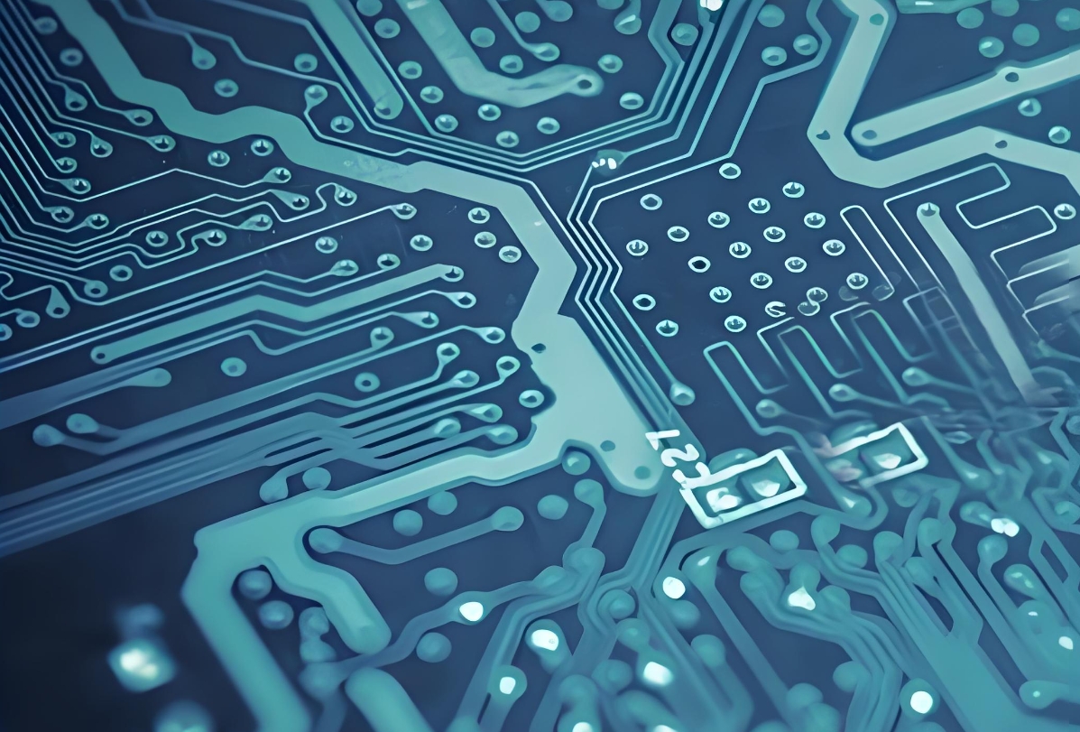
As electronic products move toward miniaturization and high performance, high-density interconnect (HDI) PCBs have become core components of modern electronic devices. HDI PCBs achieve higher signal transmission speeds and more compact designs through finer line widths, smaller apertures, and more interlayer interconnections. However, the design and manufacture of HDI PCBs also face many challenges, especially in design iteration and optimization. This article will explore the main challenges in HDI PCB design and introduce how DeepSeek uses AI technology to accelerate design iterations and help manufacturers shorten the development cycle.

Main Challenges of HDI PCB Design
1. High Wiring Complexity
The wiring density of HDI PCBs is much higher than that of traditional PCBs. Designers need to arrange more signal lines in a limited space while avoiding signal interference and crosstalk. This requires designers to have superb skills and experience, and the design cycle is long.
2. High Signal Integrity Requirements
High-frequency signal transmission places higher requirements on PCB impedance control, signal reflection, and crosstalk. The design of HDI PCB must consider signal integrity issues to ensure the stability and reliability of data transmission.
3. Difficulty in thermal management
The use of high-density wiring and high-power devices will cause the local temperature of the PCB to rise, and thermal management becomes a major problem in design. Designers need to reasonably layout heat dissipation components and optimize the heat conduction path.
4. Complex manufacturing process
The manufacture of HDI PCB involves complex processes such as micro-hole drilling, laser drilling, and electroplating hole filling. Any design defects may lead to manufacturing failure or performance degradation.
5. Long design iteration cycle
In the traditional design process, designers need to repeatedly adjust the wiring rules, optimize the layout, and verify the design effect through simulation. This process takes a long time and seriously slows down the time to market.
How DeepSeek uses AI to accelerate HDI PCB design iterations
As a leading AI technology company, DeepSeek is committed to providing intelligent solutions for the PCB industry. By applying AI technology to HDI PCB design, DeepSeek helps manufacturers significantly shorten the development cycle, reduce design costs, and improve product quality.
1. AI-driven routing rule optimization
DeepSeek has developed an AI-based routing optimization tool that can automatically analyze the design requirements of HDI PCBs and generate the optimal routing solution based on constraints such as signal integrity, thermal management, and manufacturing processes. AI tools can complete the work that traditional designs take hours or even days in just a few minutes, significantly improving design efficiency.
2. Intelligent signal integrity analysis
DeepSeek's AI algorithm can analyze signal integrity issues in PCB design in real time, such as impedance matching, reflection, and crosstalk, and provide optimization suggestions. Designers can quickly adjust design parameters to ensure the stability of signal transmission.
3. Thermal management optimization
DeepSeek's AI tool simulates the thermal distribution of the PCB, identifies hot spots, and automatically optimizes the layout of heat dissipation components. This helps improve the reliability and service life of the PCB.
4. Manufacturing process compatibility check
DeepSeek's AI system integrates a knowledge base of HDI PCB manufacturing processes, which can automatically check whether the design meets manufacturing requirements and identify potential problems in advance. This reduces the possibility of design rework and reduces manufacturing costs.
5. Fast design iteration
Through AI technology, DeepSeek achieves fast iteration of HDI PCB design. Designers can complete multiple design optimizations in a short time and verify the design effect through simulation, thereby greatly shortening the product development cycle.
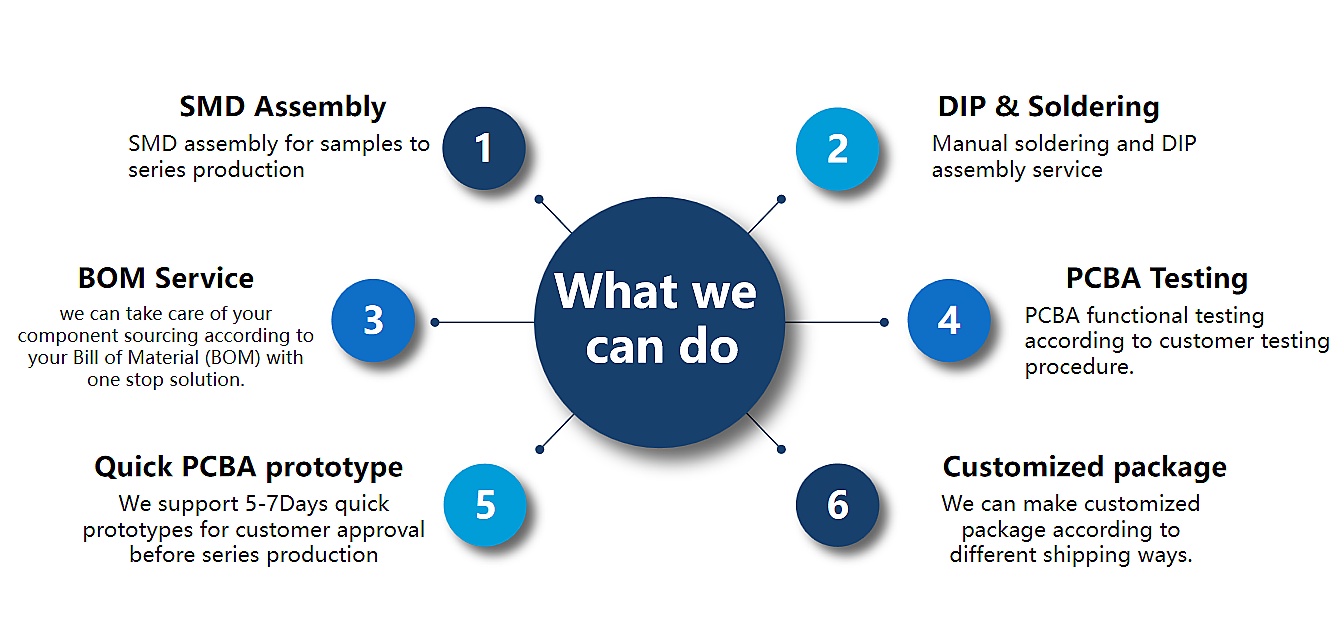
XDCPCBA: Your HDI PCB manufacturing and assembly partner
As a professional PCB manufacturer and assembly supplier, XDCPCBA is committed to providing customers with high-quality HDI PCB solutions. We provide free sample services for PCBs from 2 to 6 layers to help customers quickly verify the design. Our services include:
PCB manufacturing: using advanced HDI manufacturing processes to ensure the high performance and reliability of PCBs.
PCB assembly: providing one-stop PCBA processing services, covering the entire process from component procurement to finished product testing.
Fast proofing: supporting fast proofing and small batch production to meet the diverse needs of customers.
Technical support: providing professional technical consulting and design optimization services to help customers solve the problems in HDI PCB design.
Conclusion
The design and manufacturing of HDI PCBs are full of challenges, but through the application of AI technology, these challenges are being overcome one by one. DeepSeek's AI tools provide intelligent solutions for HDI PCB design, helping manufacturers shorten development cycles, reduce costs, and improve product quality. If you are looking for a reliable HDI PCB manufacturing and assembly partner, XDCPCBA will be your ideal choice. We provide high-quality PCB and PCBA processing services and support free sample applications. Welcome to contact us for more information!
By combining AI technology with professional manufacturing capabilities, DeepSeek and XDCPCBA are driving innovation and development in the HDI PCB industry and providing strong support for the future of electronic products!
Keywords: HDI PCB design, AI optimized wiring, signal integrity analysis, thermal management optimization, PCB manufacturing, PCB assembly, PCBA processing, free sample service, XDCPCBA, DeepSeek AI, high-density interconnect PCB, rapid design iteration, electronic product miniaturization, high-frequency signal transmission, complex PCB development, 2-6 layer PCB, PCB supplier, PCB assembly factory, printed circuit board manufacturing, PCB manufacturer, PCBA manufacturer, PCB assembly supplier, high reliability PCB, fast proofing service, one-stop PCBA solution.


