
Cracking the pain points of high-frequency PCB design: A practical guide to DeepSeek electromagnetic simulation tools
In radio frequency (RF) and microwave circuit design, the performance of high-frequency PCBs directly determines the stability and efficiency of key applications such as communication equipment, radar systems, and satellite modules. However, high-frequency circuit design faces core pain points such as poor signal integrity, complex electromagnetic interference (EMI), and time-consuming parameter optimization. This article will combine the AI-driven advantages of **DeepSeek electromagnetic simulation tool** to explore how to accelerate the parameter optimization of RF/microwave circuits, and introduce how the industry-leading XDCPCBA PCB manufacturer can help engineers break through technical bottlenecks through one-stop services (from design support to fast prototyping).

1. Core challenges of high-frequency PCB design
High-frequency circuits (usually referring to frequencies ≥1GHz) are extremely sensitive to PCB layout, material selection, impedance matching, and other links. The following problems are often faced in traditional design processes:
1. Signal integrity and crosstalk: High-speed signals are susceptible to transmission line loss, reflection, and interference from adjacent lines.
2. Electromagnetic compatibility (EMC): Complex electromagnetic field distribution leads to repeated design iterations and long debugging cycles.
3. Low efficiency of parameter optimization: Traditional simulation tools rely on manual experience adjustment, which is time-consuming and easy to fall into local optimal solutions.
2. DeepSeek electromagnetic simulation tool: AI-driven design revolution
In response to the above pain points, DeepSeek electromagnetic simulation tool significantly improves design efficiency through the deep integration of artificial intelligence algorithms and electromagnetic field modeling:
1. Intelligent parameter optimization
AI automatic parameter adjustment: Based on deep reinforcement learning (DRL), the tool can automatically adjust parameters such as transmission line width, layer spacing, and via structure to quickly approach the optimal solution.
Multi-objective trade-off: Supports simultaneous optimization of signal loss, EMI suppression and heat dissipation performance to reduce design compromises.
2. Real-time simulation and visualization
GPU accelerated computing: Compared with the traditional FDTD (finite difference time domain) method, the simulation speed is increased by more than 10 times.
3D electromagnetic field dynamic display: intuitively presents the field strength distribution in the high-frequency signal path and quickly locates the interference source.
3. Typical case: microwave filter design
A 5G base station filter needs to achieve -40dB out-of-band suppression in the 28GHz frequency band. Traditional methods require 2 weeks to iterate 10 versions of the design, while DeepSeek predicts the optimal resonant structure through AI, and only 3 simulations are required to meet the standard, shortening the development cycle by 60%.

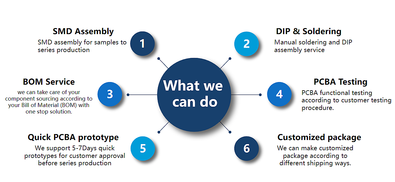
3. From design to manufacturing: XDCPCBA's one-stop service closed loop
Excellent simulation tools need to be combined with high-precision manufacturing capabilities. As an industry-leading PCB assembly supplier, XDCPCBA provides the following core support:
1. Key technologies for high-frequency PCB manufacturing
Material selection: Supply high-frequency boards such as Rogers and Taconic, with dielectric constant stability of ±0.02.
Precision processing: Line width tolerance ±0.02mm, interlayer alignment accuracy ±25μm, meeting the needs of millimeter wave circuits.
Free sample service: Free proofing of 2-6 layers of ordinary PCBs, 48-hour delivery, and support for rapid verification.
2. Core advantages of PCBA processing
RF component welding: Adopt vacuum reflow soldering process to ensure that the mounting yield of 0402/0201 package components is greater than 99.5%.
EMI protection: Built-in shielding cavity design and conductive adhesive grounding process reduce radiation interference by more than 15dB.
3. Collaborative design support
Design rule check (DRC): Provide impedance calculation tools based on manufacturing capabilities to avoid design rework.
Cost optimization suggestions: Replace high-priced special plates with stacking solutions to help customers reduce costs by 30%.
IV. Practical process: AI simulation + fast proofing implementation
Take the 77GHz automotive radar antenna board as an example to show the full-link development steps:
1. Model import: Import the antenna array element layout into DeepSeek, set the gain>15dBi, and the beam width≤10°.
2. AI simulation optimization: The tool automatically adjusts the microstrip line feed network and outputs 3 alternative solutions within 20 minutes.
3. XDCPCBA proofing verification: Select the best solution to submit a free sample order, and the actual performance error is <5% after 3 days.
4. Mass production: Based on the FR-4 mixed dielectric lamination solution, the cost of a single board is reduced by 40%, and the delivery time is compressed to 7 days.
5. Industry Trends: AI+Manufacturing Collaboratively Empowers High-Frequency PCB Innovation
With the evolution of technologies such as 6G and satellite Internet, high-frequency PCB design will face more stringent bandwidth and power consumption requirements. Through the intelligent iteration of DeepSeek electromagnetic simulation tools combined with XDCPCBA's manufacturing capabilities, engineers can focus on innovation rather than repeated trial and error, and achieve the ultimate goal of "design is production".
Act now: Visit XDCPCBA's official website to apply for 2-6 layer PCB free samples and experience AI-driven efficient development process!
**Keywords**: high-frequency PCB design, RF circuit optimization, AI electromagnetic simulation, microwave circuit parameters, PCB manufacturer, PCBA processing service, 2-6 layer PCB free samples, RF PCB assembly supplier


