Green technology leads the future: Technological trends in eco-friendly printed circuit board manufacturing and XDCPCBA's comprehensive services
In today's era of rapid technological change, the importance of printed circuit boards (PCBs) as the heart of electronic devices is self-evident. With the global awareness of environmental protection, eco-friendly PCB manufacturing technology is gradually becoming a new trend in the development of the industry. This article will explore the latest technological trends in this field and introduce XDCPCBA's comprehensive services in PCB assembly, processing and manufacturing as an industry leader.

XDCPCBA supports free PCB prototyping 2-6 layer circuit boards, PCB assembly, 2-30 layer PCB PCBA manufacturing, PCB solutions, Component Sourcing service! sales@xdcpcba.com,+8618123677761
Eco-friendly PCB manufacturing: a new chapter in green technology
Increasingly stringent environmental regulations and increasing consumer demand for sustainable products have prompted PCB manufacturers to turn to more environmentally friendly production methods. Eco-friendly PCB manufacturing not only focuses on the selection of materials, but also involves energy efficiency, waste management and pollution control in the production process. Here are some key technological trends:
Lead-free soldering technology: Lead-containing solders used in traditional PCB manufacturing have been replaced by lead-free solders to reduce harm to the environment and human health.
Biodegradable materials: Research and development of PCB substrates made of biodegradable or recyclable materials to reduce the difficulty of waste disposal.
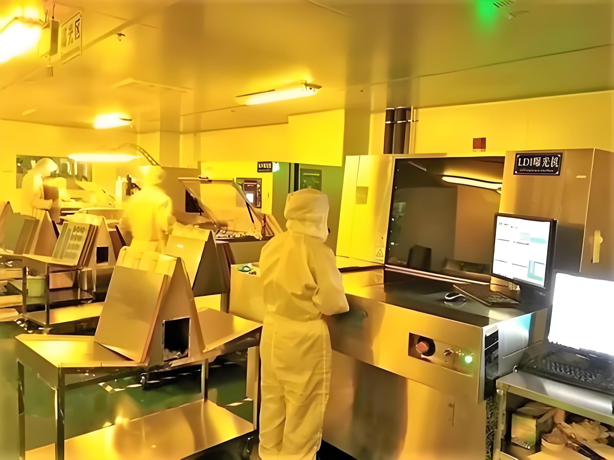
Energy-saving production equipment: Use high-efficiency and low-energy production equipment to reduce carbon emissions and improve production efficiency.
Wastewater treatment and recycling: Establish an advanced wastewater treatment system to achieve the recycling of production wastewater and reduce water waste.
Technology trend: Intelligence and miniaturization go hand in hand
With the rapid development of technologies such as the Internet of Things, 5G communications, and artificial intelligence, the design and application of PCBs are also showing a trend of intelligence and miniaturization. The application of high-density interconnection (HDI) technology, embedded component technology, and flexible PCB (FPC) makes electronic products thinner and more powerful.

HDI technology: Through micro-hole and fine line technology, high-density wiring of PCBs is achieved to meet the needs of miniaturized and high-performance electronic products.
Embedded component technology: Embed components directly into the PCB to reduce assembly steps and improve product reliability and integration.
Flexible PCB: With good bending and durability, it is suitable for electronic products that require flexible forms, such as wearable devices and smart phones.
PCB application industry fields are widely expanded
The application of PCB covers almost all electronic product fields, including but not limited to:
Communication equipment: 5G base stations, routers, switches, etc.
Consumer electronics: smartphones, tablets, smart watches, etc.
Automotive electronics: autonomous driving systems, in-car entertainment systems, sensors, etc.
Industrial control: automation equipment, intelligent manufacturing systems, monitoring systems, etc.
Medical electronics: medical equipment, health monitoring equipment, telemedicine systems, etc.
XDCPCBA: All-round PCB solution provider

As an industry-leading PCB manufacturer, XDCPCBA PCB assembly factory provides one-stop PCBA processing services, including:
PCBA processing plant: with advanced production equipment and professional technical team, providing high-quality PCBA processing services.
PCBA manufacturer: from design to production, full control to ensure product performance and quality.
Electronic contract manufacturer: Provide customized electronic manufacturing services to meet the diverse needs of customers.
SMT PCB assembly: Use surface mounting technology to achieve efficient and precise component assembly.
2-30 layer PCB manufacturer: PCB manufacturing that meets different layer requirements and supports complex circuit design.
PCB supplier: Provide stable PCB supply chain services to ensure the smooth progress of customer projects.
2-6 layer PCB free proofing service: Provide customers with free sample production services to reduce the initial development costs.
XDCPCBA is committed to driving green technology, continuously innovating technology, optimizing production processes, and providing customers with more environmentally friendly, efficient and reliable PCB solutions. Whether it is in the fields of communications, consumer electronics, automotive electronics or medical electronics, XDCPCBA is your trusted partner. Choose XDCPCBA and create a green technology future together!


