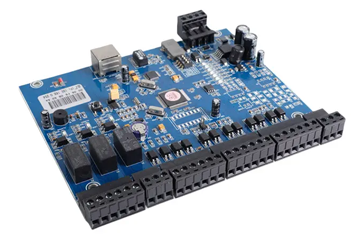
High-Speed Signal Processing in PCB Manufacturing for Servers
Servers demand PCBs capable of handling high-speed data transmission, low latency, and signal integrity across multi-gigabit interfaces like PCIe, Ethernet, and DDR memory buses. As data centers scale to support AI, cloud computing, and 5G workloads, PCB manufacturers must optimize designs to minimize crosstalk, impedance mismatches, and electromagnetic interference (EMI). This article explores advanced techniques for high-speed signal processing in server PCBs, focusing on impedance control, layer stackup optimization, and EMI mitigation strategies.
Precision Impedance Control for Multi-Gigabit Interfaces
High-speed server interfaces, such as PCIe 6.0 (64 GT/s) or 400G Ethernet, require strict impedance control to prevent signal reflections and data errors. PCBs are designed with trace geometries tailored to match the characteristic impedance of each interface—typically 85 ohms for differential pairs in PCIe or 100 ohms for Ethernet. Manufacturers use laser-direct imaging (LDI) and controlled-depth milling to maintain consistent trace widths and spacing, ensuring impedance tolerance within ±10% of the target value.
Differential pair routing is optimized to minimize skew, which occurs when signals in a pair arrive at different times due to unequal trace lengths or propagation delays. PCBs incorporate serpentine routing or phase-matching techniques to equalize trace lengths, reducing skew to less than 5 picoseconds for high-speed interfaces. For example, a DDR5 memory bus operating at 5,600 MT/s requires skew control below 2 picoseconds to maintain data validity across multiple DIMM slots.
Embedded passive components, such as resistors or capacitors, are integrated into PCB layers to terminate signals or filter noise without adding parasitic inductance. For PCIe interfaces, PCBs may include AC-coupling capacitors embedded within the substrate to block DC offsets while allowing high-frequency signals to pass. These components are placed close to connectors or ICs to minimize trace lengths and improve signal quality. Automated optical inspection (AOI) systems verify impedance-critical features during production, ensuring compliance with industry standards like IPC-2221.
Layer Stackup Optimization for Signal Integrity and Power Delivery
Server PCBs often use 12+ layer stackups to isolate high-speed signal layers from power and ground planes, reducing crosstalk and EMI. A typical stackup might allocate two outer layers for components, four inner layers for high-speed signals, and the remaining layers for power distribution and ground reference planes. Stripline routing is preferred for critical signals, as it embeds traces between two ground planes, providing better shielding than microstrip (surface-layer traces with a single ground plane).
Power integrity is equally important in high-speed server PCBs, as voltage fluctuations can degrade signal quality. Manufacturers design power distribution networks (PDNs) with low-inductance decoupling capacitors placed near high-power components like CPUs or FPGAs. For example, a server motherboard might use 0402-size ceramic capacitors with values ranging from 100 nF to 10 μF to filter noise across frequencies from 100 kHz to 1 GHz. PDN impedance is simulated during design to ensure it remains below target thresholds (e.g., <10 mΩ at 100 MHz) to prevent voltage ripple.
Backdrilling is employed to remove stubs from via holes, which can cause reflections in high-speed signals. For PCIe or Ethernet traces, PCBs use backdrilled vias with stub lengths less than 10 mils to minimize signal degradation at frequencies above 10 GHz. This process involves drilling a secondary hole slightly larger than the primary via to remove excess copper, leaving only the functional portion of the via connected to the signal layer. Backdrilling is verified using X-ray inspection to ensure complete stub removal without damaging adjacent layers.
EMI Mitigation Strategies for High-Density Server Designs
Electromagnetic interference poses a significant challenge in server PCBs due to the proximity of high-speed traces, clocks, and switching power supplies. Shielding techniques, such as embedded metal shields or conductive coatings, are used to contain EMI within specific regions of the board. For example, a PCB hosting a 100G Ethernet PHY might include a copper shield around the IC and its associated traces to block radiated emissions from interfering with adjacent memory channels.
Differential signaling is inherently more resistant to EMI than single-ended signals, as noise couples equally into both traces and cancels out at the receiver. PCBs maximize the use of differential pairs for high-speed interfaces, ensuring tight coupling (small spacing between traces) to enhance common-mode rejection. For USB 4.0 or Thunderbolt connections, differential pairs are routed with a constant spacing of 3–5 mils to maintain signal integrity in noisy environments.
Frequency-domain analysis tools are used during design to identify potential EMI hotspots, such as resonant frequencies caused by trace lengths or component placements. PCBs may incorporate frequency-selective surfaces (FSS) or electromagnetic bandgap (EBG) structures within the substrate to suppress specific EMI bands. For example, an EBG structure consisting of periodic metal patches can attenuate noise in the 1–10 GHz range, which is common in high-speed digital circuits. Manufacturers perform radiated emissions testing during production to validate that PCBs comply with regulatory standards like FCC Part 15 or CISPR 32.
By prioritizing impedance control, layer stackup optimization, and EMI mitigation, PCB manufacturers enable servers to deliver the high-speed performance and reliability required for modern data centers. These techniques ensure that server PCBs can handle escalating data rates while maintaining signal integrity in increasingly dense and complex designs.