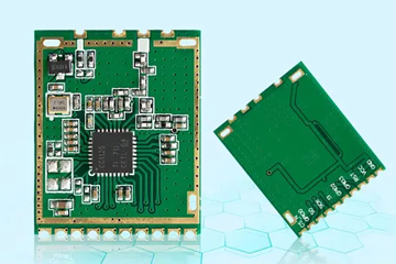
The Internet of Things (IoT) is driving an unprecedented demand for connected devices across industries such as healthcare, automotive, industrial automation, agriculture, and consumer electronics. These devices depend on Printed Circuit Board Assembly (PCB Assembly) to integrate microcontrollers, sensors, wireless modules, and power management components into compact and efficient systems.
As IoT devices become smaller, lighter, and more feature-rich, PCB Assembly processes must adapt to meet increasingly stringent requirements for miniaturization, high-density integration, and reliability. Modern IoT products often combine complex functionality with strict power efficiency and cost targets, making PCB design and assembly more challenging than ever.
Key Trends in PCB Assembly for IoT Devices
1. Increased Use of HDI, Multilayer, and Rigid-Flex PCBs
IoT devices are expected to be compact, lightweight, and multifunctional. They often need to fit inside small enclosures while integrating sensors, processors, wireless modules, memory, and power circuits on the same board. To achieve these requirements, manufacturers are increasingly adopting High-Density Interconnect (HDI), multilayer PCBs, and rigid-flex PCBs.
HDI PCBs use fine trace widths, microvias, and high wiring density, allowing for greater circuit complexity in limited space. They also provide improved signal performance by shortening the distance between components, which is critical for high-speed communication in IoT devices.
Multilayer PCBs can contain four or more conductive layers, enabling manufacturers to stack circuits vertically rather than horizontally. This not only saves space but also enhances power distribution and signal integrity, reducing electromagnetic interference (EMI) and improving overall device reliability.
Rigid-Flex PCBs combine rigid boards with flexible connectors, making them ideal for wearable devices, portable medical electronics, and compact consumer IoT products. The flexible sections allow for creative board shapes, reduced assembly steps, and better mechanical durability in devices that experience frequent movement or bending.
By leveraging these advanced PCB technologies, manufacturers can design high-performance IoT devices that are both compact and reliable, meeting the increasing demand for smaller yet more powerful electronic products.
2. High-Density SMT Assembly and Miniaturized Components
As IoT devices become more compact, the components used must also be miniaturized. Today’s IoT products commonly use ultra-small components, including 0201 and 01005 packages, fine-pitch BGAs, QFNs, and CSPs. The assembly of such tiny components requires advanced Surface Mount Technology (SMT) with extremely high precision and speed.
Modern SMT lines use:
Automated solder paste printers that ensure precise and consistent application of solder paste to achieve strong and reliable solder joints.
High-speed pick-and-place machines capable of handling thousands of components per hour while maintaining placement accuracy as fine as ±0.05 mm.
Controlled reflow ovens with carefully optimized temperature profiles to prevent solder defects such as voids, bridging, or cold joints.
To ensure product reliability, multi-stage inspection systems are implemented. AOI (Automated Optical Inspection) checks for placement accuracy and solder defects, while SPI (Solder Paste Inspection) verifies correct solder paste deposition. X-ray testing is essential for inspecting hidden solder joints, particularly for BGAs and QFNs, where visual inspection is impossible.
This combination of advanced SMT processes and inspection ensures that miniaturized IoT devices can be assembled with high first-pass yield and long-term reliability, even as designs become more complex and densely populated.
3. Integration of Wireless Communication and Power Management
Most IoT devices rely on wireless connectivity to communicate with other devices or cloud platforms. Common wireless standards include Wi-Fi, Bluetooth, Zigbee, LoRa, NB-IoT, and 5G cellular networks. These modules are often integrated alongside microcontrollers, sensors, and power management circuits, creating significant layout and assembly challenges.
Wireless modules require careful impedance-controlled routing, antenna placement, and EMI shielding to ensure strong signal transmission without interference. At the same time, IoT devices must operate efficiently to extend battery life, requiring low-power PCB designs with optimized power distribution networks.
Integrating wireless and power management components on a small PCB requires close collaboration between the design and assembly teams to prevent issues such as crosstalk, signal loss, or excessive heat generation. Manufacturers must also use multilayer PCBs and proper ground plane structures to maintain signal integrity and device stability.
As IoT applications expand into smart homes, healthcare, industrial automation, and automotive electronics, the ability to integrate multiple functions into a single compact PCB while maintaining reliability has become a key differentiator for manufacturers.
By adopting these trends—advanced PCB technologies, high-density SMT processes, and integrated wireless and power management solutions—manufacturers can meet the growing demand for powerful, compact, and energy-efficient IoT devices that perform reliably in real-world applications.

Miniaturization Challenges
The push toward smaller, more powerful IoT devices has brought significant challenges for PCB manufacturers and assemblers. As component sizes shrink and circuit density increases, every stage of the assembly process—from design to testing—becomes more complex.
1. Ultra-Small Components and Placement Accuracy
With the rise of miniaturized IoT products, components such as 0201 and 01005 packages, fine-pitch BGAs, and chip-scale packages (CSPs) are now common. Placing these components requires high-speed pick-and-place machines capable of ±0.05 mm accuracy. Even the slightest misalignment can lead to defective solder joints, weak connections, or complete device failure.
This high level of precision not only demands state-of-the-art equipment but also skilled operators and strict process control. Advanced assembly lines use automated solder paste printers and optimized reflow profiles to ensure solder quality, while AOI and X-ray systems verify placement and joint integrity. Without these measures, achieving high first-pass yield on densely populated boards would be extremely difficult.
2. Thermal Management in Compact Designs
Miniaturization limits the available surface area for heat dissipation, yet IoT devices often contain processors, wireless modules, and power management components that generate significant heat. Poor thermal design can lead to overheating, signal instability, and reduced device lifespan.
To address these issues, manufacturers must incorporate thermal vias, heat spreaders, thicker copper layers, or metal-core PCBs to improve heat transfer. In addition, strategic component placement and multilayer PCB design can help distribute heat more effectively. Achieving proper thermal management is essential for ensuring long-term reliability, particularly in industrial or automotive IoT applications that operate under harsh conditions.
3. Electromagnetic Compatibility (EMC) and Signal Integrity
IoT devices integrate multiple wireless communication modules—such as Wi-Fi, Bluetooth, Zigbee, and cellular transceivers—alongside high-speed data circuits. These components, when placed in close proximity, are prone to electromagnetic interference (EMI), which can severely affect signal quality and device performance.
To mitigate these risks, manufacturers must implement controlled impedance routing, solid ground planes, adequate isolation between analog and digital sections, and EMI shielding techniques. Proper PCB stack-up design and component placement play a critical role in maintaining signal integrity, reducing noise, and ensuring reliable wireless communication.
4. Complex Testing and Quality Assurance
As PCBs become more densely packed, accessing test points becomes increasingly difficult. Traditional inspection methods are often insufficient for verifying hidden solder joints, such as those under BGAs and CSPs.
To ensure product reliability, manufacturers rely on advanced X-ray inspection systems to check solder joint quality and detect voids or bridging issues. Functional testing and in-circuit testing (ICT) are also necessary to confirm that the assembled PCB operates correctly under real-world conditions.
Establishing a comprehensive quality control process that includes IQC, IPQC, and FQC, along with multi-stage testing, is critical for achieving high first-pass yield and long-term product reliability.
How Shenzhen Xindachang Addresses These Challenges
Shenzhen Xindachang Technology Co., Ltd. (XDCPCBA) is a leading provider of PCB manufacturing and assembly solutions, offering capabilities that specifically meet the requirements of IoT and miniaturized devices.
1. Advanced PCB Fabrication Capabilities
Supports 3 mil minimum line width/spacing, making it ideal for HDI and high-density multilayer PCB designs.
Specializes in rigid-flex PCBs and metal-core PCBs, suitable for wearables, portable devices, and high-power IoT applications.
2. High-Precision SMT and Assembly Processes
Equipped with high-speed pick-and-place machines capable of placing ultra-small components and fine-pitch BGAs with exceptional accuracy.
Uses automated solder paste printing, controlled reflow profiles, and wave/selective soldering systems for consistent assembly quality.
Provides BGA rework and X-ray inspection to ensure defect-free assembly even for hidden solder joints.
3. Comprehensive Quality Control and Testing
Implements multi-stage inspections, including IQC (Incoming Quality Control), IPQC (In-Process Quality Control), and FQC (Final Quality Control).
Uses AOI, SPI, and X-ray inspection to detect defects early and improve first-pass yield.
Offers functional testing to verify that each PCB performs as expected under real-world conditions.
4. One-Stop Turnkey Services
XDCPCBA offers PCB fabrication, component sourcing, SMT/DIP assembly, and functional testing, providing customers with a seamless, cost-effective, and time-efficient production process.


