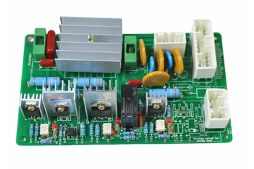
Signal Integrity Management in RF PCB Assembly: Key Considerations and Techniques
RF (Radio Frequency) PCB assemblies demand rigorous attention to signal integrity (SI) to ensure reliable performance across high-frequency bands. Unlike low-frequency designs, RF signals are susceptible to losses, reflections, and electromagnetic interference (EMI), which can degrade communication quality or cause system failures. Below are critical aspects of maintaining signal integrity during RF PCB assembly, focusing on impedance control, routing strategies, and EMI mitigation.
Impedance Control: Ensuring Consistent Signal Transmission
Impedance mismatches are a primary cause of signal reflections in RF circuits, leading to power loss and distortion. To maintain signal integrity, PCB designers must specify controlled impedance traces, which require precise management of trace width, spacing, and dielectric properties. The dielectric constant (Dk) of the PCB material plays a pivotal role here, as variations in Dk across the board can alter the characteristic impedance. Manufacturers often select materials with stable Dk values over the operating frequency range and temperature extremes to minimize fluctuations.
During assembly, soldering processes can inadvertently affect impedance if not managed carefully. For instance, excessive solder mask thickness or uneven pad coverage may alter the effective dielectric constant around traces, causing impedance deviations. DFM (Design for Manufacturability) checks should include simulations to predict how soldering and material interactions impact impedance, enabling adjustments to trace geometries or mask openings before production. Additionally, via structures used to connect layers must be designed to minimize inductance and capacitance, as these parasitic elements can disrupt impedance continuity. Back-drilling or via tenting techniques are often employed to reduce reflections at via transitions.
High-Frequency Routing Strategies: Minimizing Losses and Crosstalk
RF signal routing requires meticulous planning to avoid losses from skin effect and dielectric absorption. At high frequencies, current tends to flow near the surface of conductors (skin effect), increasing effective resistance. To counter this, designers use wider traces or embedded microstrip configurations to reduce resistance and losses. Dielectric absorption, where the PCB material temporarily stores and releases energy, can also distort signals. Selecting low-loss materials with minimal dissipation factors (Df) is crucial for maintaining signal fidelity over long distances.
Crosstalk between adjacent traces is another critical concern in RF designs. Differential pairs are commonly used to mitigate crosstalk by canceling out common-mode noise, but their effectiveness depends on precise spacing and consistent coupling. Guard traces—unused traces placed between active signals—can further isolate high-speed lines, though they must be terminated properly to avoid acting as antennas. For ultra-high-frequency applications, designers may implement co-planar waveguide (CPW) structures, which confine fields within the trace and adjacent ground planes, reducing radiation and coupling.
Electromagnetic Interference Mitigation: Shielding and Grounding Techniques
EMI can severely degrade RF performance by introducing unwanted noise into sensitive circuits. Effective shielding strategies involve enclosing noise-generating components or sections of the PCB in conductive enclosures, such as metal cans or embedded shields. These shields must be grounded at multiple points to provide a low-impedance path for EMI currents, preventing them from radiating into other areas. For flexible designs, conductive gaskets or EMI gaskets can be used to maintain shielding continuity across gaps or seams.
Grounding practices are equally vital for SI. A solid ground plane beneath RF traces reduces loop inductance and provides a reference for impedance calculations. However, ground planes must be free of splits or discontinuities, as these can create resonant cavities that amplify EMI. Stitching vias are often added to connect ground planes across layers, ensuring uniform potential and minimizing ground bounce. Decoupling capacitors placed near power pins of RF ICs further suppress high-frequency noise by shunting it to ground, but their placement and values must be optimized through simulation to avoid introducing parasitic resonances.
Material Selection and Layer Stackup Optimization
The choice of PCB materials directly impacts signal integrity in RF assemblies. High-frequency laminates with low Dk and Df values are preferred for their ability to maintain consistent impedance and minimize losses. These materials may also feature tighter thickness tolerances to reduce variations in trace geometry, which can affect impedance matching. For multi-layer boards, the layer stackup must be designed to balance signal integrity, power distribution, and thermal management. For example, placing RF signal layers between ground planes creates a stripline configuration that enhances shielding and reduces crosstalk.
Thermal expansion coefficients (CTE) of materials should also align to prevent warping during assembly, which could distort trace geometries and impedance. Hybrid stackups combining different materials for specific layers (e.g., high-frequency cores with standard prepreg) can offer cost savings without compromising SI, but they require careful modeling to ensure compatibility.
Testing and Validation for Signal Integrity Compliance
Prototyping and testing are indispensable for verifying SI in RF PCB assemblies. Time-domain reflectometry (TDR) measures impedance along traces, identifying mismatches or discontinuities that could cause reflections. Vector network analyzers (VNAs) assess insertion loss, return loss, and phase distortion across frequencies, providing insights into overall signal quality. EMI scanning tools, such as near-field probes, help locate sources of unwanted radiation, enabling targeted shielding or layout adjustments.
Iterative testing allows designers to refine the PCB layout and assembly process, addressing issues like via stubs, ground plane splits, or component placement before full-scale production. Collaboration with manufacturers during this phase ensures that assembly techniques, such as soldering profiles or cleaning processes, do not introduce SI degradation.
By prioritizing impedance control, high-frequency routing, EMI mitigation, and rigorous testing, engineers can achieve robust signal integrity in RF PCB assemblies. These practices enable reliable performance in applications ranging from wireless communication to radar systems, where even minor SI issues can have significant operational consequences.


