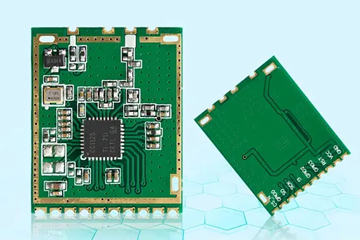
BGA Chip Soldering Process in PCB Assembly: Ensuring Reliable Connections in High-Density Designs
Ball Grid Array (BGA) chips are widely used in modern PCB assemblies due to their high pin density and compact form factor. However, their solder balls, positioned beneath the package, make visual inspection impossible and require precise process control to avoid defects like voids, shorts, or open circuits. Below are critical steps and techniques to achieve robust BGA soldering during PCB assembly.
Pre-Soldering Preparation: Cleaning and Flux Application
Surface cleanliness is paramount for BGA soldering, as contaminants like oils, fingerprints, or oxidation can inhibit wetting and lead to weak joints. The PCB pad area and BGA package undergo automated cleaning using plasma or ultrasonic systems. Plasma cleaning removes organic residues through ionized gas exposure, while ultrasonic cleaning uses high-frequency vibrations in a solvent bath to dislodge particles. For manual cleaning, isopropyl alcohol (IPA) swabs are used, followed by a deionized water rinse and dry air blow-off to eliminate residues.
Flux application follows cleaning to promote solder flow and reduce oxidation during heating. No-clean flux, which leaves minimal residue after reflow, is commonly used for BGAs to avoid post-soldering cleaning steps. The flux is applied selectively to the PCB pads using a stencil or dispensing system, ensuring even coverage without excess that could cause splattering or shorts. For fine-pitch BGAs (e.g., 0.4 mm ball pitch), the flux volume is controlled to ±10% of the target to maintain consistent wetting across all balls.
BGA package handling requires anti-static precautions to prevent electrostatic discharge (ESD) damage. Operators wear ESD-safe wrist straps and work in grounded mats, while BGAs are stored in conductive packaging until placement. Prior to soldering, the BGA is inspected for bent leads or missing balls using a 3D X-ray system or a specialized jig with magnification. Any defects are corrected by reballing the package or replacing it entirely to avoid assembly failures.
Reflow Soldering: Optimizing Temperature Profiles for BGA Reliability
Reflow soldering for BGAs involves carefully calibrated time-temperature profiles to ensure all solder balls melt and wet the pads uniformly without damaging the component or PCB. The process begins with a preheat zone (e.g., 25–150°C over 60–90 seconds) to gradually raise the temperature, activating the flux and evaporating solvents. This prevents thermal shock, which could warp the BGA or PCB, especially for large packages (>20 mm square).
The soak zone (150–180°C for 60–120 seconds) follows, allowing the entire assembly to reach thermal equilibrium. During soaking, flux reduces oxidation on the solder balls and pads, improving wetting. For lead-free solders (e.g., Sn-Ag-Cu alloys), the soak time may be extended to ensure complete flux activation, as these alloys have higher melting points (217–227°C) compared to eutectic tin-lead (183°C).
The reflow peak temperature is set 20–30°C above the solder’s melting point (e.g., 240–250°C for Sn-Ag-Cu) to ensure all balls melt simultaneously. The time above liquidus (TAL), typically 40–90 seconds, is critical: too short, and some balls may remain partially solid, causing open circuits; too long, and excessive intermetallic compound (IMC) growth can weaken joints. Nitrogen inerting in the reflow oven reduces oxidation, improving wetting and minimizing voids in the solder joints, which are later inspected via X-ray.
Post-Soldering Inspection and Rework: Detecting and Correcting Defects
Automated X-ray inspection (AXI) is the primary method for evaluating BGA solder quality non-destructively. AXI systems use 2D or 3D imaging to detect voids, misaligned balls, or insufficient wetting. For void analysis, the total void area per ball is calculated, with industry standards typically allowing ≤25% voiding for critical applications. 3D AXI reconstructs the solder joint geometry, revealing hidden defects like head-in-pillow (HiP), where a ball partially wets the pad due to thermal expansion mismatch during cooling.
Electrical testing complements X-ray inspection by verifying functional connectivity. In-circuit testers (ICT) or flying probe systems check for shorts or opens between BGA balls and adjacent traces. For high-speed designs, time-domain reflectometry (TDR) measures impedance consistency along BGA escape traces, with deviations indicating layer shift or solder joint irregularities affecting signal integrity.
Rework procedures address defective BGAs without damaging the PCB. Rework stations use localized heating (e.g., infrared or hot air) to melt the solder while protecting surrounding components with a no-clean flux-coated shield. The BGA is lifted using a vacuum pick-up tool, and the pads are cleaned of residual solder using braided copper wick or a desoldering station. A new BGA is aligned using a split-vision optical system or a jig with ±5-micron accuracy, then reflowed using the same profile as initial assembly. After rework, the joint is re-inspected via X-ray and electrical testing to confirm repair quality.
By prioritizing pre-soldering preparation, precise reflow profiling, and thorough post-soldering validation, manufacturers ensure BGA chips form reliable, long-lasting connections in PCB assemblies. These techniques address the challenges of fine-pitch designs, lead-free solders, and high-layer-count boards, enabling BGAs to meet the performance demands of advanced electronics across industries like automotive, telecommunications, and aerospace.