What are the common errors in the SMT process?
There are many common errors in the SMT (surface mount technology) process, which may come from equipment, materials, human operation and other aspects. The following are some common SMT process errors and their possible causes:
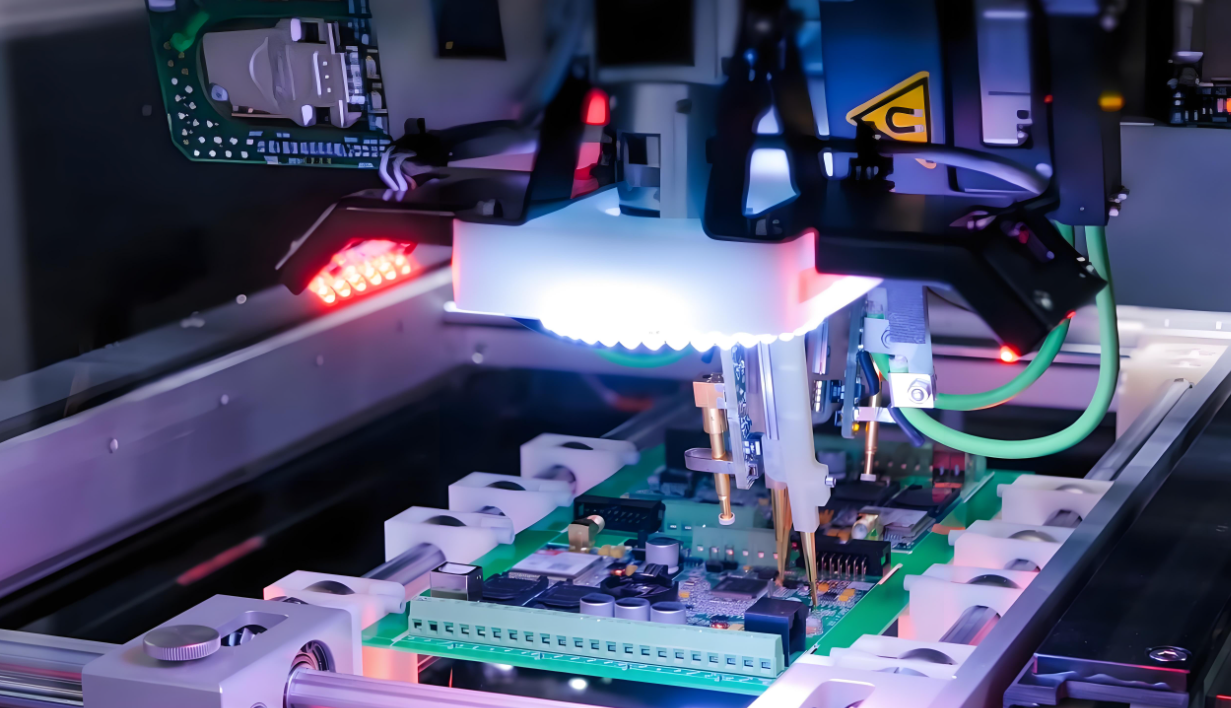
1. Component placement errors
Component placement offset
Performance: The X-Y position of the component on the PCB is offset.
Cause:
The warpage of the PCB board exceeds the allowable range of the equipment.
The height of the support pins is inconsistent, resulting in uneven support of the printed circuit board.
The suction pressure of the mounting nozzle is too low.
The program data equipment is incorrect.
The circuit board wiring accuracy is low and the consistency is poor.
The blowing pressure is abnormal during mounting.
The amount of adhesive and solder paste coating is abnormal or deviated.
Poor positioning of the substrate.
The movement of the mounting nozzle is not smooth when it rises.
The coupling between the power part and the transmission part of the X-Y workbench is loose.
The mounting head nozzle is poorly installed.
The blowing timing does not match the mounting head descending timing.
The initial data setting of the nozzle center data and the camera of the optical recognition system is poor.
Component placement angle deviation
Performance: Components rotate at an angle when they are placed.
Cause:
Support pin height is inconsistent.
Poor flatness of the workbench support platform.
PCB wiring accuracy is low and consistency is poor.
The suction pressure of the placement nozzle is too low.
The blowing pressure is abnormal during placement.
The amount of adhesive or solder paste applied is abnormal or deviated.
The program data equipment is incorrect.
The nozzle end is worn, blocked or stuck with foreign matter.
The placement nozzle does not rise or rotate smoothly.
Poor parallelism between the nozzle unit and the X-Y workbench or poor nozzle origin detection.
The optical camera is loosely installed or the data equipment is improper.
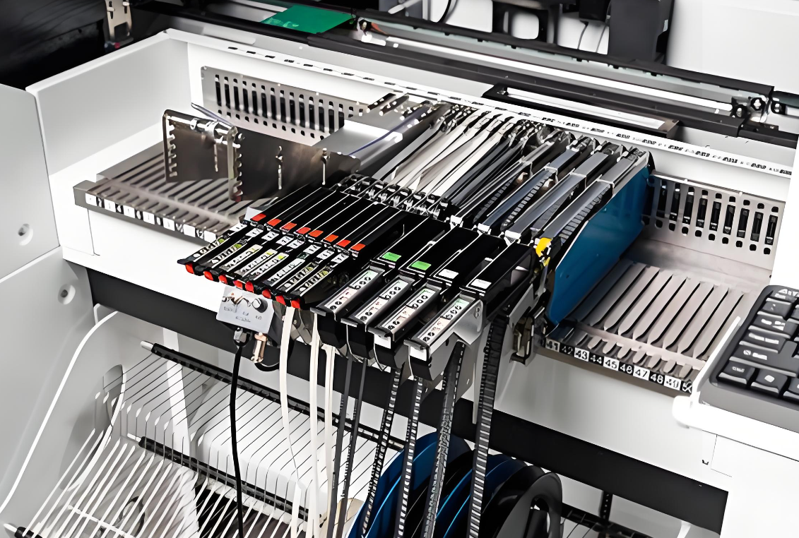
2. Component loss
Performance: Components are lost between the suction position and the placement position.
Cause:
The suction pressure of the placement nozzle is too low.
Poor posture detection sensor, wrong reference equipment.
The cleaning and maintenance of the reflector and optical recognition camera are not in place.
The tape specifications do not match the feeder specifications.
The vacuum pump is not working or the suction pressure of the suction nozzle is too low.
The plastic hot pressing tape of the tape is not peeled off or pulled up normally at the pick-up position.
The placement speed of the placement head is selected incorrectly.
The feeder is not installed firmly, the feeder ejector pin does not move smoothly, and the quick opener and closeer and the tape pressing are bad.
The paper cutter cannot cut the tape normally.
The tape cannot rotate normally with the gear or the feeder runs discontinuously.
The suction nozzle is not at the low point at the suction position, the descending height is not in place or there is no movement.
The center axis of the suction nozzle and the center axis lead of the feeder do not coincide at the pick-up position, and there is a deviation.
The suction nozzle descent time is not synchronized with the suction time.
The component thickness data device is incorrect.
The initial value of the suction height is incorrectly equipped.
3. Poor welding
Welding bridge or electrical bridge
Performance: Solder crosses two conductors that should not be electrically connected, resulting in an electrical short circuit.
Cause:
There are problems in the solder paste printing process, such as a high ratio of the template aperture to the pad and excessive solder paste deposition.
Improper reflow profile setting, such as too slow preheating zone heating rate and too long soaking time.
Uneven component placement pressure.
Electrical open circuit
Performance: Insufficient solder on the joint, resulting in an open circuit.
Cause:
Solder paste clogging the holes of the template.
Solder paste not in sufficient contact with the leads and pads.
Poor coplanarity of component leads.
Problems with the PCB manufacturing process.
Solder balls
Performance: Very tiny spherical solder particles isolated from the body that forms the joint.
Cause:
Contamination of solder paste with moisture.
Improper reflow profile.
Excessive oxide on solder powder.
Poor solder paste printing alignment.
Tombstoning effect
Performance: Chip components are partially or completely pulled off the pad to a vertical position where only one end is soldered.
Cause:
Unbalanced forces during reflow soldering.
Uneven heating.
Unequal heat sinks take heat away from the pad.
Uneven placement of components on the pad.
4. Other errors
Empty soldering: There is no soldering between the PIN pin or PAD of the part and the PAD of the PCB, resulting in a circuit failure.
Lack of tin: There is soldering between the PIN pin of the part and the PCB PAD, but the tin eating standard of the quality requirement is not met.
Rejection of soldering: There is no good soldering between the PAD/PIN of the part and the PAD of the PCB board or it cannot eat tin.
Patch offset: The position of the component is inaccurate during the patch process.
Random non-patch: The nozzle is at the low point of the patch position and the patch is not mounted and missed.
Poor posture of picking up parts: There are vertical pieces, oblique pieces, etc.
In order to avoid these errors, it is necessary to strictly control each link of the SMT process, including equipment calibration, material selection, operating specifications, etc. At the same time, strengthening quality inspection and monitoring is also an important means to ensure product quality.
XDCPCBA is a professional PCB manufacturer and PCBA processing manufacturer, focusing on providing high-quality circuit boards and assembly services for multiple industries. Our products are widely used in instrumentation, industrial control, communication equipment, automotive electronics, medical electronics, security monitoring, power appliances and consumer electronics.
In terms of PCB manufacturing, XDCPCBA provides a full range of manufacturing services from 2 to 30 layers to meet the diverse needs of customers. In particular, we also provide customers with 1-6 layers of PCB free proofing services to help customers save costs and accelerate the R&D process in the early stages of product development.
In addition to PCB manufacturing, we also provide component procurement services. With long-term cooperative relationships with many suppliers, we can provide customers with high-quality and low-cost components to ensure that customers' production needs are met.
In addition, XDCPCBA also provides one-stop PCB assembly services. From PCB manufacturing, component procurement to assembly testing, we participate in the whole process to ensure that every production link meets customer requirements and standards. Our assembly team has rich experience and advanced technology, and can provide customers with efficient and accurate assembly services.
In short, XDCPCBA is committed to providing customers with high-quality PCB manufacturing and PCBA processing services, helping customers stand out in the fierce market competition. We look forward to working with you to create a better future together.


