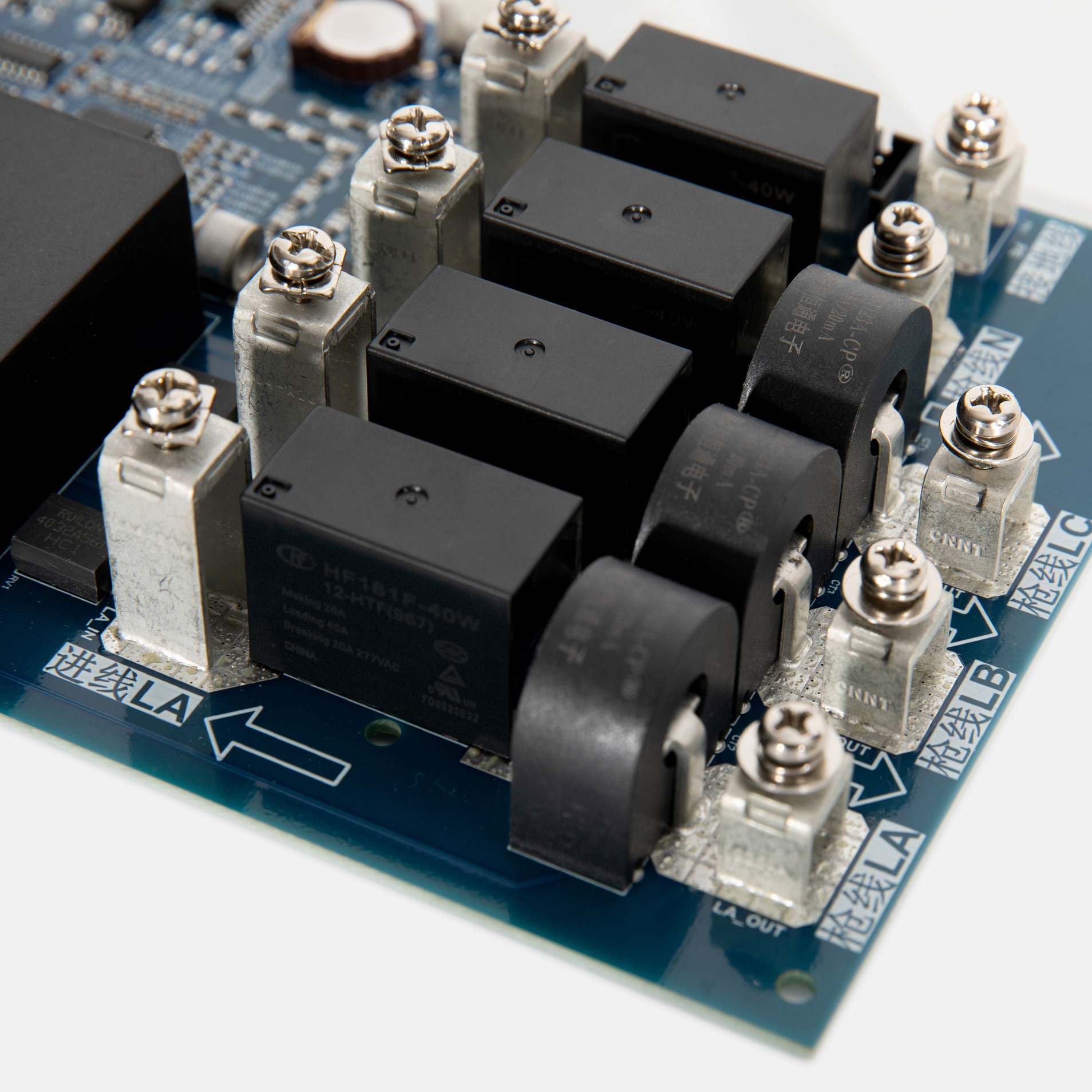
Charging pile PCBA (printed circuit board assembly) is the core component of the charging pile, and its application is extensive and vital. The following is a detailed description of charging pile PCB assembly, processing and PCBA application:
1. Charging pile PCB assembly
Charging pile PCB assembly is the process of assembling the designed PCB (printed circuit board) with other electronic components and parts. This process usually includes the following steps:
Component procurement and inspection: According to the design requirements of the charging pile, the required electronic components and parts are purchased, and quality inspections are carried out to ensure the reliability and performance of the components.
PCB board preparation: The designed PCB board is produced and necessary inspections and tests are carried out to ensure the quality of the PCB board.
Component welding: Electronic components are welded to the PCB board through automation or manual methods to form the core circuit of the charging pile.
Assembly and debugging: Assemble the welded PCB board with other components (such as housing, display, etc.), and debug to ensure that the function and performance of the charging pile meet the requirements.
2. Charging pile PCB processing
Charging pile PCB processing refers to the process of producing PCB boards, which usually includes the following steps:
Design: Design the circuit diagram and wiring diagram of the PCB according to the function and performance requirements of the charging pile.
Board making: Use professional board making equipment to make the designed circuit diagram and wiring diagram onto the PCB board.
Etching and drilling: Through chemical etching and drilling processes, the excess parts on the PCB board are removed to form circuit and component mounting holes.
Surface treatment: Surface treatment of the PCB board, such as tin plating, gold plating, etc., is performed to improve the reliability and performance of the circuit board.
Inspection and testing: Inspect and test the processed PCB board to ensure that the quality and performance of the circuit board meet the requirements.
3. Charging pile PCBA application
As the core component of the charging pile, the charging pile PCBA is mainly applied in the following aspects:
Charging control: The charging control module on the PCBA is responsible for monitoring the charging status of the battery, and adjusts the charging current and voltage according to the actual situation of the battery to ensure the safety and charging efficiency of the battery.
Communication and data processing: The communication module on the PCBA is responsible for communicating with the control system of the charging pile and transmitting charging data and information. At the same time, the data processing module is responsible for analyzing and processing the charging data to provide charging strategies and optimization suggestions.
Safety protection: The safety protection module on the PCBA is responsible for monitoring the working status of the charging pile, such as current, voltage, temperature and other parameters, and timely cutting off the power supply when an abnormality occurs to protect the safety of equipment and personnel.
User interface: The charging pile PCBA also includes a user interface module, such as a display screen, indicator light, etc., which is used to display information such as charging status and error information, so as to facilitate user operation and monitoring.
In summary, the charging pile PCB assembly and processing is an important link in the manufacturing process of the charging pile, and PCBA, as the core component of the charging pile, plays an important role in charging control, communication and data processing, safety protection and user interface.
XDCPCBA, as a leading provider in the printed circuit board (PCB) industry, offers comprehensive capabilities ranging from PCB manufacturing to PCB assembly services. With its own PCB factory, XDCPCBA specializes in producing high-quality PCBs from 2 to 30 layers, demonstrating robust production strength and a profound understanding of diverse customer needs. Furthermore, XDCPCBA launches free sample services for 2 to 6-layer PCBs, showcasing its commitment to customer satisfaction.
As a professional PCB supplier, XDCPCBA also excels as a PCBA manufacturer, providing extensive PCBA processing services within its PCB assembly factory. These services cater to various industries, including industrial automation, automotive electronics, communication equipment, the Internet of Things, mechanical equipment, instrumentation, power equipment, medical devices, aerospace, power supply electricals, household appliances, and consumer electronics.
XDCPCBA's expertise extends to various types of PCBs, such as Double-sided PCB, Multilayer PCB, High-frequency PCB, HDI PCB, Rigid-Flex PCB, Aluminum PCB, Prototype PCB, Flexible PCB, Ceramic PCB, Large size PCB, and Copper-based PCB. The company utilizes advanced technologies for PCB fabrication and assembly, ensuring precision and reliability in every product.
In addition to PCB manufacturing, XDCPCBA offers PCB design services, encompassing PCB layout design, PCB etching, and circuit board design. Customers can also benefit from prototype PCB board creation, with options for cheap PCB production and cost-effective solutions. The company understands the importance of material selection, offering a range of circuit board materials tailored to specific applications.
XDCPCBA's PCB assembly services include SMT assembly, SMD assembly, and electronic assembly, with testing and quality control measures in place to ensure the highest standards. The company's expertise in soldering circuit boards and prototype PCB assembly makes it an ideal partner for electronic manufacturin


