Efficient Design Strategies for PCB Manufacturing in Office Equipment
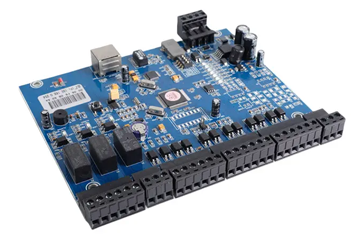
Office equipment, including printers, scanners, multifunction devices, and video conferencing systems, demands PCBs that optimize performance, power consumption, and assembly processes to meet the fast-paced demands of modern workplaces. Efficient PCB design reduces production costs, enhances reliability, and supports seamless integration with other office technologies. This article explores key strategies for achieving high efficiency in PCB manufacturing for office equipment, focusing on signal integrity optimization, thermal management, and streamlined assembly techniques.
Signal Integrity Optimization for High-Speed Data Transmission
Modern office devices rely on high-speed data interfaces like USB 3.x, HDMI, and Ethernet to handle large file transfers, 4K video streaming, and real-time collaboration. PCBs must maintain signal integrity across these high-frequency channels to prevent data corruption or latency. One approach involves using controlled impedance routing for differential pairs, ensuring consistent trace widths and spacing to match the characteristic impedance of the interface (e.g., 90 ohms for USB 3.0). Manufacturers employ advanced simulation tools during design to model signal behavior and identify potential issues like crosstalk or reflections before production.
For PCBs with multiple high-speed interfaces, layer stackup optimization is critical to minimize electromagnetic interference (EMI). Separating analog and digital ground planes reduces noise coupling, while dedicated power planes for high-current components like processors or wireless modules prevent voltage drops that could degrade signal quality. For example, a 10-layer PCB might allocate two layers for high-speed signals, two for power, and the remaining for ground and low-speed control lines. Via stitching is used to connect ground planes across layers, creating a continuous shield that suppresses EMI from external sources like Wi-Fi routers or fluorescent lighting.
Termination resistors are strategically placed near signal sources or receivers to match impedance and absorb reflections. For USB or HDMI interfaces, PCBs incorporate series resistors on differential pairs to dampen overshoot and undershoot caused by impedance mismatches. Manufacturers also use embedded passive components, such as capacitors or resistors within the PCB substrate, to save space and reduce parasitic inductance in high-speed circuits. Automated optical inspection (AOI) systems verify that trace geometries and component placements meet signal integrity requirements during assembly.
Thermal Management for Reliable Operation in Compact Designs
Office equipment often integrates multiple heat-generating components, such as processors, power regulators, and wireless modules, into compact enclosures. Effective thermal management prevents overheating, which can lead to performance throttling, component failure, or safety hazards. PCBs use thermal vias to transfer heat from surface-mounted devices (SMDs) to inner layers or the PCB’s backside, where it can dissipate through heatsinks or the device chassis. For high-power components like laser diodes in printers, PCBs may incorporate metal-core layers (e.g., aluminum or copper) to conduct heat away more efficiently than traditional FR-4 materials.
Component placement is optimized to balance thermal loads and airflow within the device. Heat-sensitive components, such as memory chips or sensors, are positioned away from hotspots like power supplies or motor drivers. For example, in a multifunction printer, the scanning module’s image sensor might be placed near an intake vent to ensure cooler operating temperatures. PCBs also use thermal simulation software to predict temperature distributions and identify potential hotspots during design, allowing adjustments to via density or component layout before prototyping.
For devices with limited airflow, such as compact all-in-one printers or video conferencing systems, PCBs incorporate phase-change materials (PCMs) or thermal interface materials (TIMs) to enhance heat dissipation. PCMs absorb excess heat during peak operation and release it slowly as temperatures drop, maintaining stable component temperatures. TIMs, such as silicone-based pads or thermal greases, improve contact between components and heatsinks, reducing thermal resistance in assemblies with uneven surfaces. Manufacturers perform thermal cycling tests during production to verify that PCBs can withstand prolonged operation without delamination or warping.
Streamlined Assembly Techniques for Cost-Effective Production
Efficient PCB assembly reduces labor costs, minimizes errors, and accelerates time-to-market for office equipment manufacturers. Design for manufacturability (DFM) principles guide PCB layout to simplify automated assembly processes. For example, components are placed in a grid-like pattern to align with pick-and-place machine nozzles, reducing repositioning time. SMDs with standardized footprints, such as 0402 or 0603 resistors and capacitors, are preferred over through-hole components to enable faster reflow soldering and reduce board thickness.
Panelization strategies optimize material usage and assembly efficiency. PCBs are grouped into panels with shared edges or breakaway tabs, allowing multiple boards to be processed simultaneously during soldering, cleaning, and testing. For high-volume production, manufacturers use v-scoring or routing to separate individual PCBs after assembly, minimizing waste and handling time. Some designs incorporate fiducial markers—small, contrasting pads placed near critical components—to guide automated optical inspection (AOI) systems in verifying solder joint quality and component alignment.
To reduce rework and scrap rates, PCBs are designed with testability in mind. In-circuit test (ICT) points are added near key components to enable electrical verification during assembly, while boundary scan (JTAG) features support debugging of complex digital circuits. For devices with firmware, PCBs may include bootloader circuits or serial programming interfaces to simplify software updates without physical access. Manufacturers also collaborate with assembly partners to implement lean production practices, such as just-in-time component delivery and real-time quality monitoring, to further enhance efficiency.
By prioritizing signal integrity, thermal management, and streamlined assembly, PCB manufacturers can produce office equipment that delivers reliable performance, energy efficiency, and cost-effectiveness. These strategies ensure that devices meet the demands of modern workplaces while remaining competitive in a rapidly evolving market.


