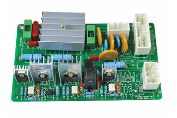
Through-Hole Technology (THT) Assembly Process and Techniques for PCB Manufacturing
While Surface Mount Technology (SMT) dominates high-density PCB assembly, Through-Hole Technology (THT) remains indispensable for components requiring mechanical strength, high power handling, or thermal dissipation. THT involves inserting component leads into drilled holes on a PCB and soldering them to pads on the opposite side, ensuring robust connections for applications like power supplies, connectors, and industrial controls. Below is a detailed breakdown of THT assembly workflows and optimization strategies to enhance reliability and efficiency.
Component Insertion: Manual vs. Automated Approaches
THT assembly begins with inserting components into pre-drilled holes on the PCB. Manual insertion is common for low-volume production or prototypes, where operators use tweezers or insertion tools to place axial-leaded resistors, diodes, or electrolytic capacitors. For radial-leaded components like ceramic capacitors, specialized fixtures may guide leads into holes to maintain alignment. Manual insertion demands operator skill to avoid bent leads, misaligned polarity, or damaged components, especially for fine-pitch parts (e.g., 2.54 mm pitch headers).
Automated insertion machines, such as radial or axial inserters, streamline high-volume THT assembly by feeding components from reels or tubes and positioning them into holes at speeds exceeding 1,000 components per hour. These systems use pneumatic or servo-driven mechanisms to ensure consistent lead insertion depth and orientation, reducing human error. For example, a radial inserter might handle electrolytic capacitors with leads spaced 5 mm apart, while an axial inserter aligns resistors along a single axis for dense layouts. Automated systems also integrate vision inspection to verify component values or polarity marks before soldering.
Component lead forming is critical for THT reliability. Leads must be trimmed to a length that ensures secure soldering without protruding excessively, which could cause shorts or mechanical stress. For axial components, leads are typically bent into a “gull-wing” or “J” shape to fit PCB layouts, with bend radii (e.g., 1–2 mm) chosen to prevent lead fracture. Radial components may require minimal forming, but leads must be straightened to ensure vertical insertion into holes. Pre-formed components from suppliers reduce assembly time but require strict quality control to avoid inconsistent lead dimensions.
Wave Soldering: Optimizing Parameters for Defect-Free Joints
Wave soldering is the primary method for soldering THT components, using a molten solder wave to wet exposed leads and PCB pads. The process involves preheating the PCB to activate flux and evaporate moisture, followed by passing the board over a solder wave generated by a pump or electromagnetic induction. Key parameters include conveyor speed (0.5–1.5 m/min), preheat temperature (100–140°C), and solder temperature (245–260°C for Sn-Ag-Cu alloys), which must be adjusted based on PCB thickness, component density, and solder type.
Flux application is crucial for wave soldering success. Water-soluble fluxes are preferred for high-reliability applications requiring post-solder cleaning, while no-clean fluxes simplify the process by leaving inert residue that does not affect electrical performance. Flux is typically sprayed or foamed onto the PCB bottom side before preheating, ensuring uniform coverage on pads and leads. Insufficient flux leads to poor wetting and solder voids, while excess flux may cause solder splatter or residue buildup.
Solder wave geometry impacts joint quality. A single-wave system uses a chip wave for fine-pitch components and a turbulent wave for larger leads, while dual-wave systems combine a laminar wave (for smooth solder flow) with a turbulent wave (to displace flux residues). For PCBs with mixed component sizes, adjusting wave height (5–8 mm) and contact time (2–4 seconds) ensures all leads are properly wetted without overheating delicate parts. Nitrogen inerting in the solder pot reduces dross formation and oxidation, improving solderability for lead-free alloys.
Post-wave soldering inspection identifies defects like solder bridges, insufficient fill, or tombstoning (where one lead lifts off the pad). AOI systems with side-view cameras detect these issues by analyzing solder fillet shapes and component alignment. For high-power applications, X-ray inspection may verify solder integrity in hidden areas, such as beneath large connectors or transformers.
Selective Soldering: Precision for Mixed-Technology PCBs
Selective soldering is ideal for PCBs combining SMT and THT components, where wave soldering is impractical due to heat-sensitive SMDs or complex layouts. This method uses a miniature solder nozzle to apply molten solder only to targeted THT leads, minimizing thermal stress on adjacent components. Selective soldering systems employ programmable X-Y tables to position the nozzle accurately, with solder flow controlled by a pump or vacuum to form consistent joints.
Nozzle design is critical for selective soldering success. Custom nozzles match the shape and size of component leads, ensuring solder wets pads without splashing onto nearby SMDs. For example, a conical nozzle might solder a single axial resistor lead, while a slot nozzle handles multiple radial leads simultaneously. Nozzle temperature (250–270°C) and dwell time (1–3 seconds) are optimized based on lead diameter and pad size to achieve proper wetting without overheating.
Flux application in selective soldering is more targeted than in wave soldering. Spray or drop-jet fluxers deposit flux only on the areas to be soldered, reducing residue and eliminating the need for cleaning in no-clean processes. For water-soluble fluxes, a controlled spray pattern ensures coverage without excess that could migrate to SMDs during heating. Flux activation temperature must align with the soldering profile to prevent premature drying or incomplete oxide removal.
Selective soldering excels at soldering difficult components like large connectors or through-hole vias near SMT parts. By isolating heat to specific areas, it avoids reflowing SMDs or warping PCBs, making it suitable for high-reliability applications like automotive or aerospace electronics. Process optimization involves iterative testing to fine-tune nozzle position, solder volume, and flux application for each component type, ensuring repeatable joint quality across production runs.
By mastering component insertion, wave soldering, and selective soldering techniques, manufacturers ensure THT assemblies meet stringent reliability standards for demanding applications. These processes complement SMT workflows, enabling efficient production of mixed-technology PCBs with robust mechanical and electrical connections.


