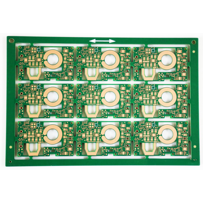
In PCB (printed circuit board) assembly, component layout optimization is a key step to ensure circuit performance, reliability, manufacturability and maintainability. The following are detailed recommendations for PCB component layout optimization:
First, the general principle
Function partition:
According to the functional blocks of the circuit, the same or related functional components are placed together to facilitate signal flow and power management.
Avoid interference between components with different functions, for example, separate digital circuits from analog circuits, and separate high-frequency circuits from low-frequency circuits.
Signal integrity:
The layout considers the direction and length of the signal line, and tries to shorten the length of the key signal line to reduce signal delay and interference.
For high-speed signal lines, differential signal transmission is adopted, and the length of the differential line pairs is shortened as far as possible, and the line pairs are kept parallel and equal in length.
Heat dissipation considerations:
Components with high thermal power consumption should be placed in a position conducive to heat dissipation, such as near vents or heat sinks.
The heating element should be evenly distributed to avoid local overheating.
Manufacturability and maintainability:
Components should be arranged to facilitate welding, testing, and servicing.
Leave enough space for test fixtures and service tools to operate.
Second, specific layout skills
Big before small, difficult before easy:
Prioritize the layout of important unit circuits and core components to ensure that their location is reasonable and signal flow is smooth.
For components that are difficult to wire, their locations should be planned in advance to avoid subsequent wiring difficulties.
Reference schematic diagram:
According to the principle block diagram of the circuit, determine the layout position of the main components, so that the signal flow is clear and reasonable.
Easy to debug and repair:
Avoid placing large components around small components to prevent obstruction during commissioning and maintenance.
There should be enough space around the components to be debugged to facilitate the connection of the test instrument.
Symmetrical layout:
The same structure of the circuit part, as far as possible to use the "symmetrical" standard layout, improve the consistency and beauty of the layout.
Component orientation is consistent:
The same type of plug-in components should be placed in one direction in the X or Y direction, and the polar discrete components of the same type should also strive to be consistent in the X or Y direction, so as to facilitate production and inspection.
Positioning of high-frequency components:
When the electrical signal exceeds the frequency of 1MHz, special attention should be paid to the positioning of high-frequency components.
High-frequency components should be as close as possible to shorten the length of the high-frequency signal line and reduce signal interference.
The ground layer must be very limited in terms of expansion, and the components connected to it should be as close to each other as possible.
Layout of decoupling capacitors:
The decoupling capacitor should be as close as possible to the power pin of the IC to shorten the loop length between the power supply and the ground and improve the decoupling effect.
Layout of cooling elements:
The heating element should be evenly distributed to avoid local overheating.
For applications with high power requirements, heating elements such as regulators and power operational amplifiers should be placed in a position conducive to heat dissipation, and the use of heat dissipation holes or heat sinks should be considered.
Avoid overlapping and crossing:
Overlap and crossover between components should be avoided to prevent short circuit and signal interference.
When wiring, the crossover of signal lines should be minimized, and vertical crossover should be used when it is unavoidable to reduce signal interference.
Make room for copper stitch:
When placing components, make sure there is enough clearance for the copper wire to pass through, especially near components with hundreds of pins.
Avoid placing too dense wiring in areas with dense components, so as not to increase the difficulty of wiring and signal interference.
Follow the schematic design:
Placing components in logical groups on the PCB layout like a schematic design will save time and minimize line length.
Many parts have been logically grouped according to the schematic diagram, and the layout should try to maintain this grouping relationship.
Third, layout inspection and optimization
Signal integrity check:
Use the signal integrity analysis tool to check the layout to ensure that the signal line length, impedance matching, crosstalk and other parameters meet the requirements.
Thermal analysis:
Thermal analysis of the PCB to ensure that the heat dissipation of the heating element is good and avoid local overheating.
Manufacturability check:
Use manufacturability inspection tools to check the layout and ensure that the layout of the components meets the requirements of the manufacturing process.
Check whether the spacing, welding points, and holes of the components meet the standards.
Optimize the layout:
The layout is optimized based on the results of signal integrity, thermal analysis and manufacturability checks.
Adjust the position, direction, spacing and other parameters of the components to make the layout more reasonable and efficient.


