Miniaturization Design in Smart Wearable PCB Manufacturing: Balancing Size, Performance, and Durability
The rapid evolution of smart wearables, including smartwatches, fitness trackers, and AR/VR glasses, has pushed PCB manufacturers to innovate in miniaturization without compromising functionality or reliability. These devices demand compact, lightweight PCBs that integrate advanced sensors, wireless connectivity, and power-efficient components while withstanding daily wear and environmental stressors. This article explores the key design strategies enabling miniaturization in smart wearable PCBs, focusing on high-density interconnect (HDI) technologies, flexible and rigid-flex architectures, and component optimization for space-constrained applications.
High-Density Interconnect (HDI) Technologies for Component Integration
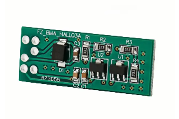
Smart wearables require PCBs capable of housing multiple components—such as microcontrollers, sensors, antennas, and batteries—within extremely limited spaces. High-density interconnect (HDI) technologies address this challenge by leveraging microvias, laser-drilled holes, and fine-pitch traces to reduce layer counts and improve signal integrity. Microvias, with diameters as small as 50 microns, enable vertical interconnections between layers, freeing up horizontal space for additional components or wider traces to handle high-current paths.
Laser-drilled blind and buried vias are particularly valuable in HDI PCBs for wearables, as they eliminate the need for through-hole vias that consume valuable real estate on both sides of the board. These vias also reduce parasitic capacitance and inductance, improving high-frequency performance for wireless communication protocols like Bluetooth Low Energy (BLE) or Wi-Fi 6. Additionally, HDI PCBs use thin dielectric materials and low-loss laminates to minimize signal attenuation, ensuring reliable data transmission between sensors and the main processor.
Another HDI innovation is the use of any-layer interconnect structures, where vias are placed anywhere on the board to create the shortest possible signal paths. This approach reduces power consumption and latency, critical for battery-powered wearables that require real-time processing of biometric data or gesture recognition. Manufacturers also employ advanced imaging techniques, such as laser direct imaging (LDI), to achieve sub-micron alignment accuracy during PCB fabrication, enabling tighter component spacing without risking short circuits.
Flexible and Rigid-Flex PCB Architectures for Ergonomic Design
Smart wearables often conform to curved or irregular body surfaces, necessitating PCBs that can bend or flex without compromising electrical performance. Flexible PCBs, made from polyimide or polyester films, provide the mechanical adaptability required for devices like smart rings or wristbands. These materials offer high tensile strength and thermal stability, allowing the PCB to withstand repeated bending cycles without cracking or delamination.
Rigid-flex PCBs combine rigid sections for component mounting with flexible sections for interconnections, offering the best of both worlds. For example, a smartwatch might use rigid layers for the processor, memory, and battery while incorporating flexible sections to route traces around the watch’s curved edges or between the main body and straps. This hybrid approach reduces the need for connectors or cables, which can add bulk and failure points, and enables seamless integration of sensors into the device’s form factor.
Designing rigid-flex PCBs for wearables requires careful consideration of bend radius requirements to prevent stress on solder joints or via barrels. Manufacturers use dynamic flex modeling tools to simulate bending scenarios and optimize trace routing in flexible zones. Additionally, coverlays or stiffeners are applied to protect flexible traces from abrasion or mechanical damage during use. For ultra-thin wearables, such as electronic skin patches, PCBs may use adhesiveless flex laminates to achieve thicknesses below 0.1mm while maintaining reliability.
Component Optimization for Space and Power Efficiency
Miniaturization in smart wearable PCBs extends beyond layout and materials to component selection and packaging. System-in-package (SiP) and chip-scale package (CSP) technologies are increasingly used to integrate multiple semiconductor dies—such as sensors, microcontrollers, and wireless modules—into a single compact unit. These packages reduce PCB footprint by eliminating the need for discrete components and interconnections, while also improving signal integrity by shortening trace lengths.
Passive components, like resistors, capacitors, and inductors, are transitioning to smaller form factors, such as 0201 or 01005 sizes, to fit into tight spaces. However, shrinking component dimensions introduces challenges in soldering and assembly, requiring manufacturers to adopt high-precision pick-and-place machines and reflow soldering profiles optimized for miniature parts. For wearables with stringent reliability requirements, such as medical-grade fitness trackers, manufacturers may use embedded passive components (EPCs) directly within the PCB substrate to eliminate solder joint fatigue risks.
Power efficiency is another critical consideration in component optimization. Smart wearables rely on low-power microcontrollers with integrated peripherals, such as ADCs for sensor interfaces and PWM controllers for LED drivers, to minimize energy consumption. Additionally, manufacturers select low-leakage MOSFETs and diodes to reduce standby power draw in always-on sensors like heart rate monitors or accelerometers. For wireless communication, power amplifiers (PAs) with adaptive bias control are used to dynamically adjust output power based on signal strength, extending battery life without sacrificing connectivity range.
As smart wearables continue to push the boundaries of miniaturization, PCB manufacturers must innovate across materials, architectures, and component technologies to deliver solutions that are both compact and capable. By leveraging HDI techniques, flexible/rigid-flex designs, and optimized components, the industry can create PCBs that enable the next generation of sleek, functional, and durable wearable devices.


