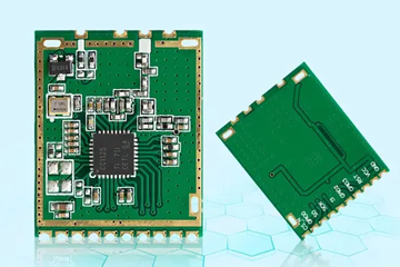
Ensuring Stability in PCB Assembly for Security and Surveillance Systems
Security and surveillance systems demand PCB assemblies that operate reliably under diverse environmental conditions, including temperature fluctuations, humidity, and electromagnetic interference (EMI). Achieving stability requires meticulous attention to material selection, thermal management, signal integrity, and manufacturing processes to prevent failures that could compromise system performance or data accuracy.
Material Selection and Environmental Resistance
The choice of PCB substrate and component materials directly impacts the assembly’s ability to withstand harsh operating environments. For outdoor surveillance applications, PCBs must resist moisture ingress and corrosion, which can degrade conductive traces or solder joints over time. High-Tg (glass transition temperature) laminates, such as FR-4 variants with improved thermal stability, are commonly used to maintain structural integrity under prolonged exposure to heat from sunlight or electronic components.
Components like connectors and sensors must also meet environmental standards, such as IP67 ratings for dust and water resistance, to ensure consistent operation in wet or dusty conditions. For PCB assemblies exposed to extreme temperatures, designers select passive components with wide operating ranges, such as ceramic capacitors instead of electrolytic ones, which can dry out or leak in high-heat scenarios. Additionally, conformal coatings applied to the PCB surface provide an extra layer of protection against moisture, chemicals, and debris, extending the assembly’s lifespan in challenging environments.
Vibration and mechanical stress are other critical factors, especially for surveillance cameras mounted on poles or moving vehicles. Rigid-flex PCBs, which combine rigid and flexible sections, reduce the risk of solder joint fatigue by absorbing vibrations and allowing controlled movement of connected components. During assembly, components are secured with underfill adhesives or potting compounds to reinforce mechanical stability and prevent disconnection due to shock or vibration.
Thermal Management Strategies for High-Performance Components
Security and surveillance PCBs often integrate power-hungry components like image sensors, processors, and wireless communication modules, which generate significant heat during operation. Effective thermal management is essential to prevent thermal runaway, where rising temperatures accelerate component degradation and lead to system failures. Heat sinks made from aluminum or copper are attached to high-power devices using thermal interface materials (TIMs), such as thermal pads or greases, to improve heat conduction away from the PCB.
For densely packed assemblies, designers incorporate thermal vias—plated holes that transfer heat from the component side to the opposite side of the PCB, where it can dissipate through larger copper areas or external heat sinks. The layout of thermal vias must consider the component’s thermal profile and the PCB’s layer stackup to avoid creating hotspots that could warp the substrate or delaminate layers. In multi-layer PCBs, dedicated thermal planes distribute heat evenly across the board, reducing localized temperature gradients.
Active cooling solutions, such as small fans or Peltier devices, are sometimes employed in enclosed surveillance systems where passive cooling is insufficient. These components require careful integration into the PCB design to ensure proper airflow and avoid introducing additional noise or vibration. Temperature sensors placed near critical components monitor thermal conditions in real time, triggering alerts or adjusting system performance (e.g., reducing frame rates in cameras) to prevent overheating without user intervention.
Signal Integrity and EMI Mitigation for Reliable Data Transmission
Security systems rely on uninterrupted data transmission, whether through wired Ethernet, wireless protocols like Wi-Fi, or cellular networks. Signal integrity issues, such as crosstalk or attenuation, can degrade video quality, delay alerts, or cause data loss, undermining the system’s effectiveness. To maintain clean signal paths, PCB designers separate high-speed digital traces from analog or power lines using dedicated ground planes and controlled impedance routing.
Differential signaling, where data is transmitted as a pair of inverted signals, is widely used to reject common-mode noise and improve immunity to EMI. This technique requires precise trace length matching and spacing to ensure synchronous signal arrival at the receiver, minimizing skew-induced errors. For wireless communication modules, antenna placement on the PCB is optimized to avoid interference from nearby components or metal enclosures, often using ground stitching or keepout zones to isolate the antenna region.
EMI shielding techniques, such as embedding conductive gaskets around sensitive components or applying metalized coatings to the PCB surface, further reduce susceptibility to external interference. Filters, such as ferrite beads or capacitors, are placed at power inputs and signal interfaces to suppress high-frequency noise generated by switching regulators or digital circuits. During testing, electromagnetic compatibility (EMC) scans identify and address sources of unwanted emissions, ensuring the PCB assembly complies with regulatory standards like FCC or CE without sacrificing performance.
Advanced Manufacturing Processes for Consistent Quality
The stability of security and surveillance PCB assemblies depends on precise manufacturing practices that minimize defects and variations. Automated optical inspection (AOI) systems scan solder joints and component placement for irregularities, such as misaligned parts or insufficient solder paste, before the assembly enters reflow soldering. This early detection prevents issues like open circuits or shorts that could cause intermittent failures in the field.
X-ray inspection is critical for evaluating solder joints beneath ball grid array (BGA) components, where visual inspection is impossible. By analyzing the internal structure of solder balls, manufacturers identify voids or cold joints that could compromise mechanical or electrical connections over time. For assemblies requiring high reliability, such as those used in critical infrastructure surveillance, burn-in testing subjects the PCB to elevated temperatures and voltages to accelerate early-life failures, ensuring only robust units are deployed.
Traceability throughout the manufacturing process enables quick identification of root causes if stability issues arise post-deployment. Each PCB is marked with a unique identifier, linking it to records of component lots, solder batch numbers, and testing results. This data-driven approach allows manufacturers to refine processes, such as adjusting reflow profiles or updating component specifications, to enhance long-term stability and reduce warranty claims.
By prioritizing environmental resistance, thermal management, signal integrity, and manufacturing precision, PCB assemblies for security and surveillance systems achieve the stability required to deliver consistent, error-free performance in mission-critical applications.


