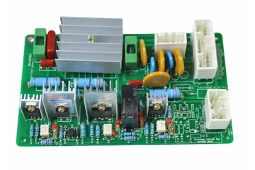
Functional Implementation in Smart Home PCB Manufacturing: Enabling Connectivity, Automation, and User Interaction
The rapid growth of smart home technology has transformed residential spaces into interconnected ecosystems where devices communicate seamlessly to enhance convenience, energy efficiency, and security. At the heart of this transformation lies the printed circuit board (PCB), a critical component that enables smart home devices to process data, execute commands, and interact with users. This article explores the key functional requirements driving PCB manufacturing for smart home applications, focusing on wireless connectivity, sensor integration, power management, and user interface design to meet the demands of modern smart living.
Wireless Connectivity and Protocol Integration
Smart home devices rely on wireless communication protocols to exchange data with central hubs, mobile apps, or other connected devices. The choice of protocol—such as Wi-Fi, Bluetooth Low Energy (BLE), Zigbee, or Z-Wave—directly impacts PCB design, component selection, and antenna placement. For instance, Wi-Fi-enabled devices require PCBs with high-frequency traces and impedance-controlled routing to support 2.4GHz or 5GHz bands, while BLE devices prioritize low power consumption, necessitating optimized antenna designs and minimal signal loss.
Antenna integration is a critical aspect of wireless PCB design. Manufacturers use embedded antennas, such as planar inverted-F antennas (PIFAs) or chip antennas, to save space and reduce costs. These antennas must be carefully positioned to avoid interference from metallic components or high-current traces. For multi-protocol devices, PCBs may incorporate switchable antenna paths or dual-band antennas to support seamless switching between networks.
Security is another consideration in wireless connectivity. PCBs for smart home devices must include hardware-based encryption modules or secure elements to protect data transmission from eavesdropping or tampering. This involves integrating cryptographic accelerators, true random number generators (TRNGs), and secure boot mechanisms into the PCB design to ensure end-to-end security for user credentials and device commands.
Sensor Integration for Environmental Awareness
Smart home devices leverage an array of sensors to monitor environmental conditions, detect motion, or recognize user presence. PCBs must accommodate these sensors while maintaining signal integrity and minimizing power consumption. Common sensors include temperature/humidity sensors, ambient light sensors, PIR (passive infrared) motion detectors, and ultrasonic range finders. Each sensor type imposes specific design constraints, such as analog signal conditioning circuits for temperature sensors or shielded traces for ultrasonic sensors to prevent noise interference.
Multi-sensor fusion is a growing trend in smart home PCBs, where data from multiple sensors is combined to improve accuracy and context awareness. For example, a smart thermostat might integrate temperature, humidity, and occupancy sensors to adjust heating/cooling settings dynamically. PCB designers must ensure that sensor outputs are synchronized and calibrated, often incorporating microcontrollers with built-in analog-to-digital converters (ADCs) to process raw sensor data before transmission to the cloud or local hub.
Low-power design is essential for battery-operated sensors, such as door/window contacts or leak detectors. PCBs for these devices use low-leakage components, sleep modes, and energy harvesting techniques (e.g., solar or piezoelectric) to extend battery life. Additionally, manufacturers optimize PCB layouts to reduce parasitic capacitance and inductance, which can drain power or distort sensor readings in high-precision applications.
Power Management for Energy Efficiency and Reliability
Smart home devices operate in diverse power scenarios, ranging from mains-powered appliances like smart lights to battery-driven sensors and always-on hubs. PCBs must incorporate robust power management systems to handle these variations while ensuring stability and efficiency. For mains-powered devices, PCBs include AC-DC converters with high power factor correction (PFC) to meet regulatory standards and reduce energy waste. These converters are often designed with isolated topologies to protect users from electrical shocks.
Battery-powered devices demand ultra-low-quiescent-current (IQ) power management ICs (PMICs) to maximize battery life. PCB designers optimize component placement to minimize trace lengths between the battery, PMIC, and load, reducing voltage drops and power losses. Additionally, PCBs may include fuel gauge circuits to monitor battery health and provide accurate remaining capacity estimates to users via mobile apps.
Energy harvesting is an emerging area in smart home PCB design, particularly for devices deployed in hard-to-reach locations. PCBs for solar-powered sensors or kinetic energy harvesters incorporate DC-DC boost converters to step up low-voltage inputs to usable levels. These circuits must be highly efficient to operate with minimal energy input, often requiring careful selection of inductors and capacitors with low equivalent series resistance (ESR) to minimize losses.
User Interface Design for Intuitive Interaction
While many smart home devices are controlled remotely via mobile apps, local user interfaces remain essential for quick adjustments or status checks. PCBs for devices with physical interfaces—such as smart thermostats, locks, or switches—must integrate touch sensors, LED indicators, or capacitive buttons while maintaining a sleek, modern aesthetic. Touch-enabled PCBs use projected capacitive technology (PCT) or self-capacitance sensors to detect finger proximity, with traces arranged in a grid pattern to map touch locations accurately.
Haptic feedback is another feature gaining traction in smart home interfaces, providing tactile confirmation of user actions. PCBs for haptic-enabled devices include piezoelectric actuators or linear resonant actuators (LRAs) driven by dedicated drivers to generate vibrations. These components must be positioned to avoid interference with other sensitive circuits, such as wireless antennas or microphones.
Accessibility is a key consideration in user interface design, particularly for aging-in-place or assistive living applications. PCBs for voice-controlled devices, such as smart speakers or displays, incorporate multi-microphone arrays with beamforming capabilities to capture user commands clearly in noisy environments. Noise-cancellation algorithms are implemented in digital signal processors (DSPs) on the PCB to filter out background sounds and improve speech recognition accuracy.
As smart home technology continues to evolve, PCB manufacturers must adapt to support increasingly complex functionalities while balancing cost, size, and power constraints. By focusing on wireless connectivity, sensor integration, power management, and user interaction, the industry can deliver PCBs that form the backbone of intelligent, responsive, and user-friendly smart home ecosystems.


