Introduction
Design for Manufacturability (DFM) is critical to ensure that a PCB design can be efficiently produced. By following the right PCB DFM rules, designers can reduce errors and costs. In this article, we will discuss the key DFM rules that streamline the transition from design to production, helping you create high-quality, cost-effective PCBs.
The Essential PCB DFM Rules
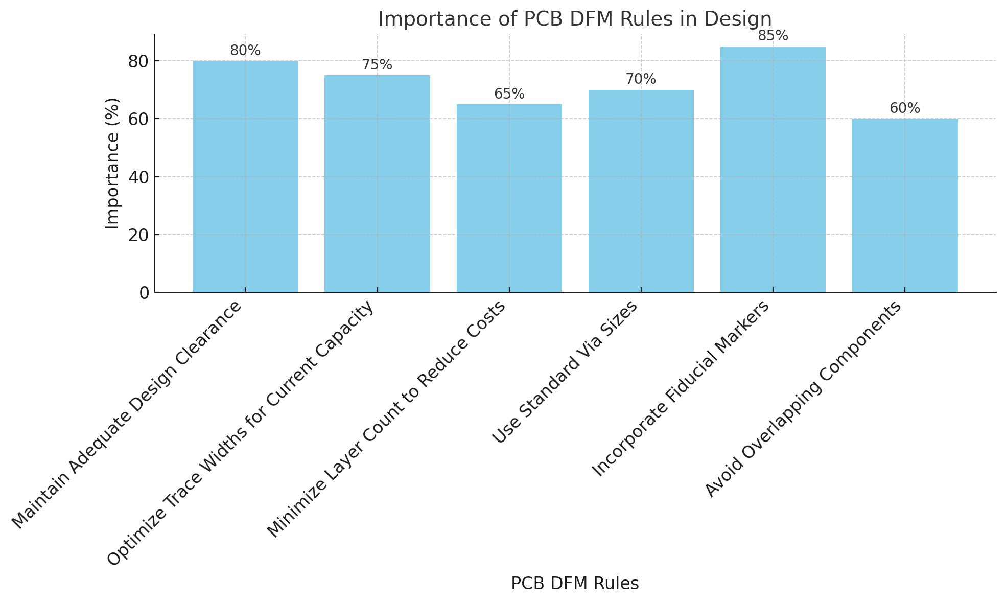
Maintain Adequate Design Clearance
Maintaining proper clearance between components, traces, and pads is one of the foundational PCB DFM rules. Adequate spacing prevents short circuits, manufacturing defects, and assembly issues that may arise due to crowded layouts. By following the manufacturer’s minimum clearance specifications, designers can ensure that the board’s electrical performance is optimized, and assembly processes remain seamless.
Optimize Trace Widths for Current Capacity
The width of traces directly impacts the ability of a PCB to handle electrical current without overheating. When designing a PCB, trace widths should be calculated based on the expected current load, ensuring that each trace can support the necessary power requirements. Overly narrow traces may lead to overheating, while wider traces, typically used for power circuits, ensure better current distribution and reliability. This optimization ensures that PCBs perform as expected in real-world conditions.
Minimize Layer Count to Reduce Costs
One of the most effective cost-saving strategies in PCB design is minimizing the number of layers used. The more layers a PCB has, the more complex and costly the manufacturing process becomes. By reducing the number of layers while maintaining the integrity of the design, manufacturers can reduce production costs and complexity. This approach not only makes the process more affordable but also improves the design's manufacturability.

Key Design Considerations for Effective PCB DFM
Use Standard Via Sizes
Using standard via sizes is another crucial PCB DFM rule that impacts both manufacturing time and cost. Non-standard vias can significantly slow down production and increase costs, especially when complex drilling techniques like microvias or blind/buried vias are required. Stick to commonly used via sizes unless your design explicitly requires specialized vias for high-density designs.
Incorporate Fiducial Markers
Fiducial markers are essential for automated optical inspection (AOI) and assembly. These markers ensure that the layers are correctly aligned and help pick-and-place machines position components with high accuracy. Incorporating fiducial markers ensures a smoother and more reliable assembly process, reducing errors during the manufacturing phase.
Avoid Overlapping Components
To optimize automated assembly, it is critical to avoid overlapping components. Overlapping pads or insufficient spacing between components can cause issues during the soldering process, leading to defects such as solder bridges. Proper spacing ensures that components are easily placed, and the assembly process is efficient, preventing costly manufacturing errors.
Managing Drilling and Via Design in PCB DFM
Drill Size and Annular Ring Rules
Proper drill size and annular ring specifications are vital for ensuring that vias and pads are well-aligned during PCB fabrication. Drilling issues, such as misaligned vias or insufficient annular rings, can lead to poor connectivity or unreliable electrical performance. Following standard drill size rules and ensuring proper annular ring dimensions helps avoid these problems, leading to more reliable and manufacturable PCBs.
Drill Type | Minimum Drill Size | Minimum Annular Ring Size | Recommended Annular Ring Size |
Standard Drill | ≥ 0.3 mm | ≥ 0.15 mm | ≥ 0.25 mm |
Microvias | ≤ 0.2 mm | ≥ 0.10 mm | ≥ 0.15 mm |
Via Tenting for Solderability and Reliability
Tenting vias, or covering them with a solder mask, is especially important for ensuring the reliability of high-density designs. Vias near sensitive components can lead to issues like solder wicking, which compromises the integrity of the solder joints. Proper tenting of vias reduces these risks and improves the overall performance and reliability of the PCB.
Via Type | Tenting Requirement | When to Tent |
Small vias | Tented | Close to SMD pads to prevent solder bridging |
Large vias | Tent, cap, and fill | For vias under components like BGAs or QFNs |
Blind/Buried | Tented or filled as needed | For reducing exposure and improving soldering |
Proper Drill-to-Copper Clearance
Ensuring adequate drill-to-copper clearance is critical for the structural integrity of the PCB. Insufficient clearance can cause copper traces to become exposed, leading to potential short circuits or damage during production. By adhering to the recommended clearance values, manufacturers can prevent these issues and ensure that the PCB maintains optimal electrical performance throughout its lifecycle.
Component Placement and Soldering for PCB DFM
Place Components for Easy Automated Assembly
Effective component placement is key to facilitating automated assembly. Components should be placed in a manner that aligns with the capabilities of pick-and-place machines, ensuring that they can be easily and accurately placed without manual intervention. By optimizing component placement, manufacturers can reduce errors and improve assembly efficiency, which ultimately results in lower production costs.
Component Spacing and Orientation
Maintaining consistent spacing between components and ensuring proper orientation is vital for soldering accuracy. Adequate spacing helps avoid solder bridges, while uniform orientation ensures that all components are correctly placed during the assembly process. These practices prevent defects, such as misalignments or unintentional short circuits, that can arise from poorly spaced or oriented components.
Optimizing Solder Mask Coverage
Solder mask coverage is another essential aspect of PCB DFM. The solder mask ensures electrical isolation between traces and pads and prevents solder bridges during the assembly process. Proper mask coverage also improves the overall reliability of the PCB by minimizing the chances of unintended solder connections. Ensuring that there is adequate solder mask clearance around SMT pads is vital for reducing the risk of defects during manufacturing.
Best Practices for PCB DFM in High-Speed and High-Density Designs
Controlled Impedance Design for High-Speed Circuits
For high-speed PCB designs, maintaining controlled impedance is crucial for signal integrity. When designing for high-speed circuits, it is essential to collaborate with fabricators to ensure proper stack-up and impedance control. This ensures that signals are transmitted accurately, minimizing errors and ensuring reliable performance in high-frequency applications.
Minimize Crosstalk and Signal Interference
Crosstalk and signal interference can significantly affect the performance of high-speed circuits. To minimize these issues, PCB designers must carefully manage trace spacing and implement solid ground planes and return paths. By optimizing these elements, designers can ensure that the PCB maintains excellent signal integrity and reduces electromagnetic interference (EMI).

How to Test DFM Compliance Before Manufacturing
Automated DFM Checks
Before sending PCB designs to production, performing automated DFM checks is essential to ensure that the design adheres to manufacturing standards. These checks identify issues such as improper trace-to-trace clearance, missing solder mask, or component placement violations. Running these checks helps catch potential issues early, reducing the risk of costly delays or rework.
Review Manufacturing Constraints Early
Consulting with manufacturers early in the design process is critical for identifying potential design issues that may affect manufacturability. By reviewing the constraints and discussing the design with the manufacturer before production begins, designers can ensure that the design meets the necessary requirements, minimizing the chances of delays or production failures.
DFM Checkpoint | Description |
Trace Width and Spacing | Ensure minimum trace width and spacing as per manufacturer specs. |
Drill Sizes and Annular Ring | Check the drill sizes and ensure proper annular ring size. |
Component Spacing | Maintain proper distances between components for assembly. |
Solder Mask Coverage | Ensure correct solder mask clearance to prevent solder bridges. |
Silkscreen Positioning | Avoid overlapping silkscreen and ensure proper polarity markings. |
Conclusion
Adhering to PCB DFM rules is key to ensuring designs are manufacturable and cost-effective. Best practices for clearance, trace widths, and component placement help create reliable, production-ready PCBs. Collaborating early with manufacturers and using DFM tools can prevent costly errors. By integrating DFM principles, designers achieve faster production, lower costs, and higher quality. For optimal results, working with companies like XDCPCBA ensures smooth, efficient manufacturing, delivering cost-effective and reliable PCBs.
FAQ
Q: What are PCB DFM rules?
A: PCB DFM rules ensure that a PCB design is optimized for manufacturability, reducing production errors and costs. They cover aspects like trace width, clearance, and component placement.
Q: Why are PCB DFM rules important?
A: PCB DFM rules help streamline the transition from design to production, ensuring that the design is manufacturable, reliable, and cost-effective.
Q: How do PCB DFM rules reduce manufacturing costs?
A: By following PCB DFM rules, designers avoid costly production errors, reduce material waste, and optimize the design for quicker, more efficient manufacturing.
Q: How do I apply PCB DFM rules in my design?
A: Follow best practices such as maintaining adequate design clearance, optimizing trace widths, and minimizing layer count to ensure your PCB is both manufacturable and cost-effective.
Q: What are common mistakes to avoid with PCB DFM rules?
A: Common mistakes include insufficient clearance between components, improper trace widths, and not considering manufacturing constraints early in the design process.


