Introduction
Multi-layer PCBs (Printed Circuit Boards) are crucial for modern electronics. They are composed of multiple layers that handle complex functions in a compact design. This article explores the multi-layer PCB manufacturing process, highlighting design, assembly, testing, and the benefits of these advanced boards. You'll learn how multi-layer PCBs are created, their significance in electronics, and the challenges faced during their production.
Understanding Multi-Layer PCBs
What Are Multi-Layer PCBs?
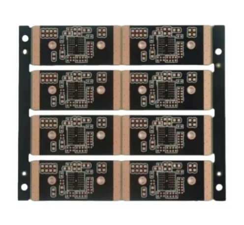
Multi-layer PCBs are circuit boards that consist of three or more layers of conductive copper foil, separated by insulating layers. These boards allow for more compact designs, with components packed into multiple layers, making them suitable for complex electronic devices like smartphones, laptops, and medical equipment. Unlike single-layer or double-layer PCBs, which only have one or two conductive layers, multi-layer PCBs can have anywhere from four to 48 layers, depending on the complexity of the design.
Feature | Multi-Layer PCB | Single-Layer PCB | Double-Layer PCB |
Number of Layers | 3 or more layers | 1 layer | 2 layers |
Design Complexity | High (more layers and vias) | Simple (one conductive layer) | Moderate (two conductive layers) |
Performance | High performance, low EMI, compact | Limited performance, basic tasks | Moderate performance |
Applications | Complex electronics, high-speed | Simple consumer devices | Moderate complexity devices |
Cost | Expensive | Low cost | Moderate cost |
Why Are Multi-Layer PCBs Important?
Multi-layer PCBs are crucial for modern electronics as they enable more circuits to be placed in a smaller area. The layered structure not only saves space but also improves signal integrity by reducing the path length for signals and providing better shielding for high-frequency signals. They are also capable of handling more complex designs and are often used in high-performance applications, such as high-speed computing and automotive systems.
The Multi-Layer PCB Manufacturing Process
Design Phase and Pre-Production Preparation
The design phase is critical for successful multi-layer PCB manufacturing. Engineers use specialized software to create the layout, define the routing, and determine the number of layers required. The design must also meet certain manufacturability standards, which is why Design for Manufacturability (DFM) checks are essential to ensure the design can be produced without issues. Once the design is finalized, it is converted into Gerber files, which act as the blueprint for the manufacturing process.
Material Selection and Layer Bonding
Choosing the right materials is essential for the performance of multi-layer PCBs. The base material is usually FR-4, a fiberglass-reinforced epoxy laminate, but other materials like Rogers or Teflon are used for high-frequency applications. After the base material is selected, copper foil is laminated onto it to form the conductive layers. The layers are then bonded together with prepreg sheets, which are layers of resin that provide insulation between the conductive copper layers.
Material | Purpose | Common Uses |
FR-4 (Fiberglass Epoxy) | General-purpose, cost-effective base | Consumer electronics, computers |
Rogers (PTFE) | High-frequency applications, low signal loss | High-speed circuits, RF designs |
Teflon | Low dielectric constant, minimal loss | Satellite and telecom devices |
Inner Layer Processing and Etching
In the next step, the inner layers are processed by applying a photosensitive layer that reacts to UV light. The design pattern is transferred to this layer, and then the unwanted copper is etched away. The remaining copper traces form the circuit. This step is followed by Automated Optical Inspection (AOI) to check for defects such as shorts or open circuits.
Drilling and Via Formation
Drilling is an essential step for creating vias, which are tiny holes that connect the different layers electrically. Multi-layer PCBs often use different types of vias, such as through-hole vias, blind vias, and buried vias. Each via type requires precise drilling to ensure proper alignment. Laser drilling is commonly used to ensure accuracy when drilling vias as small as 0.05 mm.
Laminating and Final Layer Processing
After the inner layers are processed, they are stacked together with insulating materials (prepreg) and bonded under high heat and pressure in a process known as lamination. The laminated stack forms the core of the multi-layer PCB. Once laminated, the outer layers are processed using the same etching techniques to create the final circuit pattern.
Step | Description | Importance |
Design and Pre-Production | Layout, routing, and layer stack-up; DFM checks | Ensures manufacturability and reduces errors |
Material Selection | Choosing copper foils, prepreg sheets, and laminates | Critical for performance and durability |
Inner Layer Processing | Etching and photolithography to create circuit patterns | Defines the electrical pathways |
Lamination | Bonding layers using heat and pressure | Ensures structural integrity |
Drilling and Via Formation | Drilling holes for vias and interconnecting layers | Key for electrical connections |
Challenges in Multi-Layer PCB Manufacturing
Misalignment and Precision Issues
One of the challenges in multi-layer PCB manufacturing is maintaining precise alignment during the lamination process. Even slight misalignment between the layers can result in signal disruptions, short circuits, or poor performance. Ensuring proper layer alignment requires sophisticated equipment and careful handling during manufacturing.
Drilling and Via Issues
Maintaining precision during drilling is another challenge. Since multi-layer PCBs require vias to interconnect the layers, any misalignment or improper drilling can lead to broken vias or unreliable electrical connections. Moreover, copper plating inside the vias must be done accurately to ensure proper conductivity across layers.
Via Type | Description | Common Usage |
Through-Hole Via | Passes through all layers of the PCB | Standard for interconnecting layers |
Blind Via | Connects outer layers to inner layers | Used for compact designs with high-density layers |
Buried Via | Connects two or more inner layers without visible holes on the outer layers | Used in high-density and complex PCBs |
High-Cost and Complexity
Due to the intricate nature of multi-layer PCB manufacturing, these boards are more expensive to produce than single or double-layer PCBs. The increased complexity, longer production time, and need for specialized equipment contribute to the higher cost of multi-layer PCBs.

Benefits of Multi-Layer PCBs
Compact Design and High Performance
Multi-layer PCBs allow for higher component density in a smaller space. This compact design is especially beneficial for modern electronic devices like smartphones and laptops, where space is limited, but performance cannot be compromised. By stacking multiple layers, designers can fit more components into a smaller area without sacrificing functionality.
Improved Signal Integrity and EMI Shielding
Multi-layer PCBs provide excellent signal integrity by reducing the distance between components and minimizing interference. The internal layers can be dedicated to power and ground planes, which help reduce electromagnetic interference (EMI) and enhance the overall performance of high-speed circuits.
Durability and Reliability
The multi-layer construction makes these PCBs more durable and able to withstand thermal and mechanical stresses. This is crucial for applications in demanding industries like automotive, aerospace, and medical devices, where reliability and longevity are paramount.
Advantages | Challenges |
Compact Design | More layers lead to higher manufacturing costs |
Improved Signal Integrity | Increased design complexity and longer production time |
Durability and Reliability | Requires precise drilling and alignment |
High Performance | Requires specialized equipment and skilled labor |
Multi-Layer PCB Testing and Quality Control
Testing Methods for Multi-Layer PCBs
Testing is critical to ensure multi-layer PCBs meet performance standards. Common testing methods include In-Circuit Testing (ICT) for checking for shorts or open circuits, and Functional Testing to ensure the board performs as expected. Additionally, Flying Probe Testing is used for smaller batch production, while Automated Optical Inspection (AOI) helps identify visual defects.
Ensuring Reliability and Performance
To ensure reliability, multi-layer PCBs undergo rigorous thermal and electrical testing to check for heat tolerance, signal integrity, and other performance factors. Industry standards such as IPC-6012 ensure that the PCB meets the necessary reliability requirements for demanding applications.

Applications of Multi-Layer PCBs
Consumer Electronics
Multi-layer PCBs are widely used in consumer electronics like smartphones, tablets, and wearables. These devices require compact and high-performance PCBs, and multi-layer designs allow for increased functionality without increasing size.
Automotive and Aerospace Applications
In the automotive and aerospace industries, multi-layer PCBs are used for sensors, navigation systems, and other critical components. Their durability and reliability make them ideal for harsh environments where performance is crucial.
Medical Devices
Multi-layer PCBs are essential in medical devices like pacemakers, X-ray machines, and heart monitors. Their compact design and high reliability make them perfect for use in life-saving equipment that demands precision and longevity.
Conclusion
Multi-layer PCBs are essential in modern electronics, offering compact and high-performance solutions. Their manufacturing process is intricate, but the advantages they provide in high-speed, high-density applications are indispensable. Understanding the multi-layer PCB process helps businesses make informed decisions, ensuring optimal performance. Partnering with the right manufacturer, like XDCPCBA, guarantees the success and reliability of your designs.
FAQ
Q: What is a multi-layer PCB?
A: A multi-layer PCB is a printed circuit board made of three or more layers of conductive material, designed for compact and high-performance electronic devices.
Q: Why are multi-layer PCBs necessary in electronics?
A: Multi-layer PCBs enable high-density circuits, improved signal integrity, and compact designs, making them essential for modern devices like smartphones and computers.
Q: How are multi-layer PCBs manufactured?
A: Multi-layer PCBs are created through a complex process that involves layer stacking, bonding, etching, drilling, and surface processing to ensure high functionality.
Q: What are the benefits of multi-layer PCBs?
A: Multi-layer PCBs provide advantages like smaller size, better performance, reduced electromagnetic interference (EMI), and increased durability for advanced electronics.
Q: What is the cost difference between multi-layer PCBs and single-layer PCBs?
A: Multi-layer PCBs are more expensive due to their complexity and additional layers, but they offer better performance and are essential for high-speed, compact devices.


