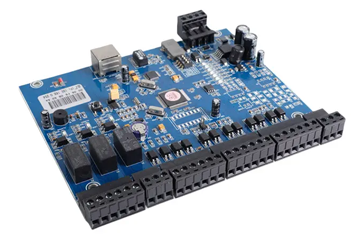
Reliability Design in Industrial Control PCB Manufacturing: Ensuring Long-Term Performance in Harsh Environments
Industrial control systems, such as those used in factory automation, energy management, and transportation infrastructure, demand PCBs (Printed Circuit Boards) capable of operating reliably for decades under extreme conditions. Unlike consumer electronics, industrial PCBs must withstand temperature fluctuations, vibration, humidity, electrical noise, and chemical exposure without failure. This article explores the key reliability design principles in industrial control PCB manufacturing, focusing on material selection, thermal management, mechanical stability, and electrical robustness to meet the stringent demands of industrial applications.
Material Selection for Durability and Chemical Resistance
Industrial environments expose PCBs to corrosive substances, moisture, and abrasive particles, making material selection critical for long-term reliability. Standard FR-4 laminates, widely used in commercial applications, may degrade under prolonged exposure to chemicals or humidity, leading to delamination or electrical leakage. Instead, manufacturers opt for high-performance laminates such as polyimide, PTFE (Polytetrafluoroethylene), or ceramic-filled composites, which offer superior resistance to moisture absorption, chemical corrosion, and thermal aging.
For PCBs used in outdoor or marine settings, conformal coatings or parylene layers are applied to protect against salt spray, condensation, and dust. These coatings form a thin, impermeable barrier that prevents moisture ingress and reduces the risk of short circuits. Additionally, manufacturers select solder masks with high abrasion resistance to withstand mechanical wear from vibrating components or frequent maintenance activities.
Another consideration is the compatibility of materials with cleaning processes. Industrial PCBs often require rigorous cleaning to remove flux residues or contaminants accumulated during operation. Water-soluble solder masks and no-clean flux formulations are preferred to simplify cleaning and minimize the risk of chemical interactions that could weaken dielectric properties over time.
Thermal Management Strategies for High-Power Applications
Industrial control PCBs frequently handle high currents and voltages, generating significant heat that can degrade components or cause thermal runaway if not properly managed. Effective thermal management begins with the PCB layout, where designers prioritize heat dissipation through optimized trace routing, copper pours, and thermal vias. Wide traces with low resistance are used for power paths to minimize I²R losses, while dedicated copper planes act as heat sinks to distribute heat evenly across the board.
Thermal vias are strategically placed beneath high-power components, such as MOSFETs or inductors, to transfer heat to inner layers or external heatsinks. These vias are often filled with thermally conductive epoxy or solder to enhance thermal conductivity. For PCBs in enclosed environments with limited airflow, manufacturers incorporate embedded thermal pads or metal-core substrates (MCPCBs) to improve heat dissipation without relying on external cooling systems.
Material selection also plays a role in thermal performance. High-Tg (glass transition temperature) laminates with Tg values above 170°C are used to prevent warping or delamination under thermal stress. Additionally, manufacturers avoid materials with high coefficients of thermal expansion (CTE), which can cause micro-cracking in solder joints or via barrels during temperature cycling. Instead, low-CTE materials like ceramic-filled PTFE or Rogers laminates are chosen to maintain dimensional stability over wide temperature ranges.
Mechanical Stability Design for Vibration and Shock Resistance
Industrial equipment, such as motors, pumps, or conveyor systems, generates constant vibration and occasional shocks that can damage PCBs if not properly designed. To enhance mechanical stability, manufacturers use rigid-flex PCB architectures that combine rigid layers for component mounting with flexible sections to absorb vibrations. The flexible portions act as shock absorbers, reducing stress on solder joints and vias during mechanical disturbances.
Component placement is another critical factor. Heavy components, such as transformers or electrolytic capacitors, are positioned close to the PCB’s center of gravity to minimize rotational forces during vibration. Additionally, manufacturers avoid placing components near PCB edges or cutouts, where stress concentrations are highest. For through-hole components, staking or adhesive bonding is used to prevent movement or fatigue in high-vibration zones.
Solder joint reliability is paramount in vibration-prone environments. Manufacturers adhere to IPC-A-610 standards for soldering quality, ensuring void-free joints with sufficient fillet heights. For surface-mount devices (SMDs), reflow soldering profiles are optimized to create strong intermetallic bonds between pads and components. In extreme cases, underfill epoxy is applied beneath BGAs (Ball Grid Arrays) or QFNs (Quad Flat No-Leads) to reinforce solder joints and prevent cracking under repeated stress.
Electrical Robustness Design for Noise Immunity and Signal Integrity
Industrial control PCBs operate in electrically noisy environments filled with electromagnetic interference (EMI) from motors, relays, or power supplies. To ensure reliable operation, designers implement shielding techniques such as dedicated ground planes, stitching vias, and EMI gaskets to block external noise. For high-speed signals, controlled impedance traces are used to maintain signal integrity, with precise calculations for trace width, spacing, and dielectric thickness to achieve target impedance values (e.g., 50Ω or 100Ω).
Power integrity is equally important, as voltage drops or ripple can disrupt sensitive analog or digital circuits. Manufacturers use decoupling capacitors placed close to power pins of integrated circuits (ICs) to filter out high-frequency noise and stabilize voltage levels. For PCBs with mixed-signal designs (analog and digital circuits), isolation techniques like optocouplers or transformers are employed to prevent crosstalk between noisy digital sections and sensitive analog components.
Testing and validation are integral to electrical robustness. PCBs undergo EMI/EMC testing to verify compliance with standards like IEC 61000-4-6 (conducted immunity) and IEC 61000-4-3 (radiated immunity). Signal integrity is assessed using time-domain reflectometry (TDR) or vector network analyzers (VNAs) to detect impedance mismatches or reflections that could degrade performance.
As industrial automation and smart manufacturing continue to advance, PCB manufacturers must prioritize reliability design to meet the evolving demands of industrial control systems. By focusing on material durability, thermal management, mechanical stability, and electrical robustness, the industry can produce PCBs that deliver consistent performance in the most challenging industrial environments.


