Selective Wave Soldering in PCB Assembly: Key Advantages for Modern Electronics Manufacturing
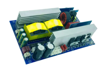
Selective wave soldering has emerged as a critical solution for PCB assemblies requiring precision, reliability, and compatibility with mixed-technology designs. Unlike traditional wave soldering, which processes entire boards, selective soldering targets specific through-hole components (THCs) or areas, minimizing thermal stress and enabling higher-density layouts. This article explores its advantages in reducing thermal damage, enhancing process flexibility, and improving solder joint quality for complex assemblies.
Minimizing Thermal Stress on Sensitive Components
One of the most significant challenges in PCB assembly is protecting temperature-sensitive components like MEMS sensors, electrolytic capacitors, and plastic-bodied connectors from thermal shock. Traditional reflow or wave soldering exposes entire boards to high temperatures, risking warping, delamination, or functional degradation. Selective wave soldering addresses this by isolating heat to targeted areas, ensuring adjacent SMT components or delicate parts remain unaffected.
For example, a PCB with a high-power resistor requiring through-hole soldering alongside a temperature-sensitive IC can be processed without exposing the IC to reflow temperatures. By using a localized solder nozzle, only the resistor’s leads interact with the molten solder, while the rest of the board stays at ambient temperature. This approach is particularly valuable for automotive electronics, where reliability under extreme conditions is non-negotiable.
Additionally, selective soldering reduces the need for thermal shielding materials like Kapton tape or silicone pads, which can leave residue or complicate inspection. The precision of nozzle-based soldering ensures consistent heat application, eliminating uneven thermal expansion that might cause micro-cracks in ceramic components or solder joint fatigue over time.
Enhanced Flexibility for Mixed-Technology Assemblies
Modern PCBs often combine surface-mount technology (SMT) and through-hole components to leverage the strengths of both. Selective wave soldering excels in such scenarios by allowing manufacturers to solder THCs after SMT reflow without damaging previously placed parts. This sequential process eliminates the need for costly dual-reflow setups or manual soldering, streamlining production for high-mix, low-volume applications.
For instance, a medical device PCB with fine-pitch SMT ICs and large power connectors can be assembled in two stages: first, reflowing the ICs, then selectively soldering the connectors using a programmable nozzle. This flexibility also supports prototyping and rapid iteration, as engineers can modify THC placement without redesigning the entire soldering process.
The technology’s adaptability extends to board geometries. Unlike traditional wave soldering, which requires uniform component heights for consistent wave contact, selective soldering accommodates uneven surfaces by adjusting nozzle height and solder flow dynamically. This capability is crucial for assemblies with embedded components or 3D-stacked PCBs, where traditional methods would struggle to achieve reliable connections.
Improved Solder Joint Quality and Reduced Defects
Selective wave soldering offers superior control over solder volume, wetting time, and flux application, directly translating to higher joint reliability. By using a focused solder stream, the process ensures consistent fillet formation without the risk of bridging or solder splatter common in traditional wave soldering. This precision is particularly beneficial for high-density connectors or fine-pitch THCs, where even minor defects can lead to electrical failures.
The ability to customize flux deposition further enhances quality. Unlike global flux spraying in conventional methods, selective soldering applies flux only to targeted areas, reducing residue buildup and simplifying post-process cleaning. This targeted approach also minimizes voiding in solder joints, as the controlled solder flow displaces air pockets more effectively than a broad wave.
For critical applications like aerospace or military electronics, selective soldering’s repeatability and traceability are invaluable. Process parameters such as nozzle temperature, dwell time, and solder alloy composition can be logged and adjusted for each assembly, ensuring compliance with stringent quality standards like IPC-A-610.
Lower Rework Rates and Material Waste
Traditional wave soldering often generates defects like tombstoning, insufficient solder, or damaged components, requiring costly rework. Selective soldering’s precision drastically reduces these issues by eliminating variables like uneven pad sizes or misaligned components that affect entire boards. For example, a misplaced THC can be resoldered individually without scrapping the entire PCB, saving time and material costs.
The technology also minimizes solder waste by using only the amount needed for specific joints. In contrast, traditional wave soldering consumes excess solder to maintain wave stability, leading to higher dross generation and material costs. Selective systems often incorporate solder recovery mechanisms, further reducing environmental impact and operational expenses.
Compatibility with High-Complexity Designs
As PCBs evolve toward smaller form factors and higher component densities, selective wave soldering provides a scalable solution for assembling intricate layouts. Its ability to solder components in tight proximity without thermal interference supports designs with minimal spacing between THCs and SMT parts. This is particularly advantageous for wearables, IoT devices, and advanced computing hardware, where space constraints are severe.
The process also accommodates non-standard component shapes, such as irregularly shaped connectors or heat sinks, by using custom nozzles or soldering paths. This adaptability ensures manufacturers can address evolving design requirements without investing in entirely new soldering equipment.
By combining thermal precision, process flexibility, and defect reduction, selective wave soldering has become indispensable for high-reliability PCB assemblies. Its ability to handle mixed-technology designs, complex geometries, and sensitive components positions it as a cornerstone of modern electronics manufacturing, driving efficiency and quality across industries.


