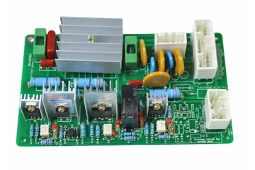
In PCB manufacturing, the design and implementation of green oil Bridges (also known as solder mask Bridges or solder mask DAMS) are crucial links to ensure electrical isolation between surface mount device (SMD) pads and prevent short circuits during soldering bridging. The following elaborates in detail from aspects such as design specifications, implementation processes, common problems and optimization measures:
First, the design specifications for the green oil bridge
Size requirements
Conventional design: The width of the green oil bridge usually needs to be ≥6 mils (0.152mm) to ensure the feasibility of the manufacturing process. For instance, for a 1oz thick copper substrate, when using green ink, the minimum bridge width can be controlled at 4mil, while for the mixed color ink, it needs to be ≥5mil.
High-density design: When the pad spacing is less than 0.2mm (such as in LQFP48 packaging), LDI (Laser Direct Imaging) technology should be combined to optimize the solder mask bridge width to 0.1mm (4mil) to avoid the risk of detachment.
The relationship between pad spacing and solder mask window opening: When the pad spacing is 8mil, a single side window opening of 2mil can retain a 4mil solder mask bridge. If the pad spacing is 0.35mm (approximately 14mil), a solder mask bridge can be fabricated by default. If the value exceeds this limit, solder mask window opening should be adopted as an alternative.
Process adaptability
Exposure technique selection:
Traditional CCD exposure machine: Due to the large alignment tolerance, the solder mask window is usually 0.05mm (2mil) larger than one side of the pad, resulting in a reduction in the width of the solder mask bridge.
LDI exposure machine: It can achieve precise 1:1 solder mask and pad window opening, reducing the width of the solder mask bridge to 0mm (theoretical value), but in practice, the minimum process width (such as 0.1mm) needs to be retained.
Copper thickness and ink type: For thick copper substrates (2-4 oz), the width of the bright black ink solder mask bridge needs to be increased to ≥6mil to compensate for the development error. Green ink, due to its high technological maturity, can achieve more precise bridge width control.
Special scene processing
Gold finger area: It is strictly prohibited to set up a green oil bridge. A whole block of solder mask should be used to cover it to prevent the green oil bridge from falling off during plugging and unplugging.
Large copper surface area: The width of the tin barrier bridge should be ≥8mil to prevent tin bridging during wave soldering.
Second, the realization process of the green oil bridge
Negative film development process
After applying the solder mask ink, the area to be retained is cured through ultraviolet exposure, and the unexposed part is developed and removed to form a window.
For multi-layer boards, the solder mask window and the circuit pads can be strictly designed to be of equal size, while for single-layer boards, engineering compensation is required to ensure the accuracy of the bridge width.
Control of key process parameters
Exposure time: Adjust to 11-12 stops to ensure the curing effect of the solder mask layer.
Developing parameters: The developing concentration is controlled at 0.8-1.2%, the temperature range is 28-32℃, the developing pressure is 2-2.5Kg/cm², and the speed is 45-50% at the exposed copper point.
Pretreatment optimization: The IS pumice powder grinding plate machine is used for pretreatment, and its green oil adhesion effect is superior to that of the Universe nylon brush plate belt chemical treatment machine.
Low-temperature tunnel parameters: Adjust the temperature and time to ensure that the solder mask is fully cured and does not deform.
Third, common problems and optimization measures
The green oil bridge fell off
Reasons: The width of the solder mask bridge is too small (such as <4mil), the copper thickness does not match, excessive development, etc.
Measures: When optimizing the design, increase the width of the solder mask bridge, select the appropriate type of ink and copper thickness, and strictly control the developing parameters.
Serve the green oil on the plate
Reasons: Alignment error, insufficient exposure, incomplete development, etc.
Measures: Use a 10x magnifying glass to assist in alignment, increase exposure time, and optimize the developing process.
Short circuit risk
The reason is that the solder mask bridge is missing or insufficient in width, causing the solder to flow and form a conductive bridge.
Measures: When the pad spacing is small, give priority to retaining the solder mask bridge. If it cannot be achieved, the pad layout needs to be optimized through DFM (Design for Manufacturability) analysis.
Fourth, collaborative optimization between the design end and the manufacturing end
Design-end considerations
Download the chip data sheet and confirm the pin spacing and edge spacing. For example, the center pitch of the pins of the STM32F103c8t6 chip is 0.5mm and the edge pitch is 0.2mm.
Adjust the expansion width of the solder mask according to the technological level of the board factory. For instance, Jialichuang multi-layer boards adopt LDI technology, which can reduce the spread width of the solder mask to increase the width of the solder mask bridge.
Use DFM tools (such as Huaqiu DFM) to conduct gap analysis, identify solder mask bridge areas below 4mil, and generate optimization suggestions.
Manufacturing-end capability matching
Confirm the exposure technology (CCD or LDI) and ink type used by the board factory to ensure that the design parameters match the manufacturing capacity.
For extreme cases (such as when the solder mask bridge fails to meet the minimum width requirement), it is advisable to consider changing the chip package type or adjusting the pad spacing.


