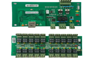
Testing is a critical part of the circuit board assembly (PCBA) process. Once the components are soldered onto the PCB, they must undergo rigorous testing to ensure that they function as expected and meet quality standards. Testing helps identify potential defects early, preventing costly repairs or replacements. This article will explore the various types of tests performed on assembled PCBs, why they are necessary, and how they contribute to the overall quality assurance process. By using these methods, manufacturers can ensure that their PCBs are reliable, high-performing, and ready for use in end products.
1.The Importance of PCB Testing
Before shipping assembled PCBs to customers or using them in products, it's essential to ensure that they function as intended. PCB testing helps identify potential defects or malfunctions early, preventing costly repairs or replacements later. These tests confirm the functionality, reliability, and durability of the boards, ensuring that they meet design specifications and can withstand real-world conditions.
PCB testing is especially important for industries like consumer electronics, automotive, medical devices, and telecommunications, where reliability and performance are critical. Testing also helps detect manufacturing defects, such as solder bridges, misplaced components, or damaged circuits, which can render a PCB non-functional.
2.Types of Testing Performed on Assembled PCBs
There are several testing methods available to verify the quality and functionality of an assembled PCB. The types of tests performed depend on the complexity of the design, the intended application, and the level of reliability required. Common testing methods include:
Visual Inspection
Automated Optical Inspection (AOI)
In-Circuit Testing (ICT)
Functional Testing
Burn-In Testing
Each of these tests plays a specific role in ensuring that the PCB is defect-free and ready for use in the final product.
3.Visual Inspection
Why Visual Inspection is the First Step
Visual inspection is often the first step in the PCB testing process. It involves a manual or automated review of the assembled PCB to check for visible defects. Technicians or machines inspect the board for issues such as soldering defects, misplaced components, scratches, and board warping.
What Issues Are Identified Through Visual Inspection?
While visual inspection can't catch every problem, it is effective in identifying common issues, including:
Solder Bridges: Where solder has accidentally connected two adjacent pads or traces.
Missing Components: If a component has been overlooked during assembly or is improperly placed.
Component Damage: Any visible signs of damage to components, such as cracked capacitors or burnt resistors.
Incorrect Component Placement: If components are misaligned or incorrectly oriented.
While visual inspection can be done by hand, it is often performed using automated systems that are faster and more accurate in detecting surface-level issues.
4.Automated Optical Inspection (AOI)
What is Automated Optical Inspection (AOI)?
Automated Optical Inspection (AOI) is a widely used technique for inspecting PCBs after assembly. AOI utilizes high-resolution cameras to capture detailed images of the PCB and compare them to a reference design or pre-programmed rules. The system identifies defects such as soldering issues, misaligned components, and improper placements.
How AOI Detects Defects
AOI works by scanning the assembled PCB and identifying discrepancies between the actual image and the expected design. The system can detect:
Soldering Defects: It can identify cold joints, where solder does not properly connect the component and PCB pad, and insufficient soldering, where too little solder is applied.
Misalignment: It ensures that components are placed in the correct position and orientation.
Component Issues: AOI detects problems like missing components, incorrect part numbers, or damaged components.
AOI is an essential tool in modern PCB assembly lines, as it provides fast and accurate detection of potential issues, significantly reducing manual inspection time.

5.In-Circuit Testing (ICT)
What is In-Circuit Testing (ICT)?
In-Circuit Testing (ICT) is one of the most thorough methods for testing PCBs. It checks the functionality of individual components and ensures that all electrical connections are correctly established. ICT uses a bed of needles that make contact with specific test points on the PCB, testing for short circuits, open circuits, and proper component functionality.
Why is ICT Important?
ICT plays a crucial role in ensuring that all electrical connections on a PCB are intact. Some key features of ICT include:
Short Circuit Detection: Identifies any unintended connections between traces or components, preventing malfunction or failure of the PCB.
Open Circuit Detection: Ensures that all circuits are properly connected and that no component or trace is incomplete or broken.
Component Testing: Verifies that each component functions as expected. For instance, it checks resistors, capacitors, and integrated circuits for the correct resistance, capacitance, or voltage.
ICT is particularly useful for high-density or complex PCBs, as it can detect even the smallest electrical issues, ensuring that the assembled PCB is fully operational.
6.Functional Testing
What is Functional Testing?
Functional testing is a type of testing that checks whether the PCB performs as intended under real-world conditions. While ICT ensures the electrical integrity of the PCB, functional testing verifies that the entire assembly works according to its specifications.
Examples of Functional Testing
Functional testing may include several specific checks, such as:
Power Functionality: Ensures the PCB powers up correctly and performs basic operations.
Signal Integrity: Tests the PCB’s ability to send and receive signals as designed, crucial for communication-related devices like smartphones and computers.
Voltage Checks: Verifies that voltage levels are correct at various test points across the PCB.
Performance Testing: Confirms that the PCB performs the intended tasks, such as controlling a motor, processing signals, or interacting with other devices.
Functional testing is essential for ensuring that the final PCB behaves as expected in its intended environment.
7.Burn-In Testing
What is Burn-In Testing?
Burn-In Testing is a process where the PCB is subjected to stress conditions such as higher voltages, temperatures, or longer operation times to detect any early failures. The goal of burn-in testing is to identify components that might fail prematurely under normal use.
Why is Burn-In Testing Used?
Burn-in testing is often performed on high-reliability products, such as those used in aerospace, medical, or military applications. This test helps ensure the long-term stability and reliability of the PCB by detecting any components that might have manufacturing defects or those that are more likely to fail soon after initial use. The testing conditions may simulate real-world stresses, including overvoltage, overcurrent, and high temperatures.
While burn-in testing is not necessary for all products, it is essential for those requiring high reliability or used in critical applications.
FAQs – Related Questions
How does Automated Optical Inspection (AOI) detect defects in PCBs?
AOI uses high-resolution cameras to scan the PCB, comparing the actual layout to a reference design. It identifies defects such as soldering issues, misaligned components, and other faults like missing or incorrect parts. The system flags any discrepancies between the actual and expected designs, making it an essential tool for catching defects early in the assembly process.
What is the difference between in-circuit testing (ICT) and functional testing?
ICT focuses on testing the electrical connections and the functionality of individual components, detecting issues like short circuits and open circuits. It ensures that each component is properly connected and operates as intended. Functional testing, however, evaluates the overall performance of the PCB in real-world conditions, verifying that the board performs its intended function, such as voltage checks, signal integrity, and power functionality.
Is burn-in testing necessary for every PCB assembly?
No, burn-in testing is not required for every PCB. It is mainly used for high-reliability products where failure could have catastrophic consequences, such as medical or aerospace devices. Burn-in testing is effective for detecting early failures in critical components that may degrade over time. This test helps ensure long-term reliability, especially for boards used in demanding applications.
Can I perform all types of testing in-house, or should I rely on external services?
Basic tests, like visual inspection and functional testing, can often be done in-house, depending on your resources and equipment. However, more complex tests such as AOI and ICT require specialized equipment and expertise, so these are usually handled by external testing services. Before deciding, assess your in-house capabilities and whether outsourcing to a professional service will save time and ensure more accurate results.
Conclusion
Testing is an essential part of the circuit board assembly process, ensuring that the final product meets the highest standards of quality, performance, and reliability. Methods such as visual inspection, Automated Optical Inspection (AOI), In-Circuit Testing (ICT), functional testing, and burn-in testing play crucial roles in identifying potential issues early in the process. These testing methods help prevent defects, ensuring that the PCB functions as intended and improves its long-term reliability and longevity.
For manufacturers, conducting thorough testing not only reduces the risk of returns but also significantly enhances customer satisfaction by providing a reliable, defect-free product. It also ensures that the product is ready for deployment, meeting the specific requirements and functioning as expected in real-world conditions. By selecting the appropriate combination of tests tailored to each application, manufacturers can streamline the assembly process, reduce unnecessary delays, and ultimately deliver high-quality, reliable products to their customers with confidence.


