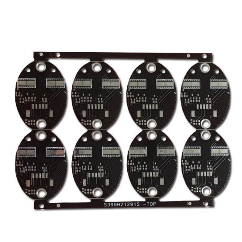
As a world-leading metal substrate manufacturer, XDCPCBA focuses on the high-precision R&D and production of aluminum substrates (Aluminum PCB) and copper substrates (Copper PCB), providing efficient heat dissipation and reliable performance guarantee for high-power equipment such as LED lighting, power modules, automotive electronics, and 5G communications. The company is equipped with advanced processes such as vacuum pressing, laser grooving, and lead-free tin spraying, supporting aluminum layer thickness of 1-3mm, copper layer thickness of 1-10OZ (35-350μm), and thermal resistance as low as 0.3℃·in⊃2;/W, meeting the heat dissipation needs of different power levels from 5W to 500W.
I. Core technology and application of aluminum substrate**
1. **Material and structural innovation**
- **High thermal conductivity aluminum alloy substrate**: Using 6061-T6 aviation-grade aluminum alloy, the thermal conductivity is 180W/m·K, which is more than 20 times higher than the traditional FR4 substrate.
- **Three-layer structure design**: copper foil (1-3OZ) + insulation layer (0.05-0.3mm) + aluminum substrate, withstand voltage ≥500V DC, insulation resistance >10^10Ω.
- **Lightweight design**: optional thickness of 0.8-3mm, suitable for portable devices and lightweight scenarios.
2. **Precision manufacturing process**
- **Line accuracy**: minimum line width/line spacing 4mil/4mil, through-hole aperture 0.3mm, support high-density LED array layout.
- **Surface treatment**:
- Chemical immersion gold (ENIG): nickel layer ≥3μm, gold layer 0.05-0.1μm, antioxidant capacity increased by 3 times.
- Lead-free tin spraying (HASL): thickness 3-5μm, suitable for wave soldering process, welding yield >99.8%.
- **Special process**:
- Laser grooving (accuracy ±10μm) to achieve special-shaped structure cutting
- Anodizing treatment enhances the corrosion resistance of the substrate
3. **Typical application scenarios**
- **LED lighting**:
- High-power street lamp aluminum substrate (2mm thick, supporting 100W LED)
- Plant growth lamp substrate (integrated reflective coating design)
- **Industrial power supply**:
- Inverter aluminum substrate (thickness 1.6mm, integrated shielding layer)
- Electric welding machine control board (DBC process copper-aluminum composite substrate)
- **Consumer electronics**:
- Wireless charger substrate (ultra-thin 0.8mm design)
- Projector heat dissipation module (partial buried copper block structure)
II. Core technology and breakthrough of copper substrate**
1. **Material and process advantages**
- **High thermal conductivity composite material**:
- 94HB copper clad laminate with ceramic filling technology, thermal conductivity 2.5W/m·K
- Buried copper block/copper pillar design, local heat dissipation efficiency increased by 50%
- **Advanced manufacturing process**:
- DBC (direct copper bonding) process: copper layer and ceramic substrate bonding strength > 40MPa, temperature resistance up to 800℃
- AMB (active metal brazing) process: achieve metallurgical bonding of copper layer and Al₂O₃ ceramic
- **Multi-layer structure design**:
- 2-6 layer hybrid structure (rigid layer + metal layer)
- Ultra-thin copper substrate (0.4mm) supports foldable flexible connection
2. **Precision manufacturing parameters**
- **Line accuracy**: minimum line width/line spacing 3mil/3mil, micropore aperture 0.2mm
- **Impedance control**: differential impedance tolerance ±8%, support 50Ω/100Ω standard impedance
- **Reliability verification**:
- Hot and cold shock (-55℃~+125℃, 1000 cycles)
- Pad peel strength>1.5N/mm (IPC-6012 Class 3)
3. **Industry application cases**
- **Automotive electronics**:
- Motor controller copper substrate (10OZ copper layer, temperature resistance 120℃)
- New energy battery BMS substrate (integrated temperature sensor)
- **5G communication**:
- Base station RF power amplifier copper substrate (thermal resistance 0.5℃·in⊃2;/W)
- Optical module heat dissipation substrate (supporting 25Gbps PAM4 signal)
- **Medical equipment**:
- MRI equipment high-power coil substrate (DBC process)
- Extracorporeal lithotripter control board (high-voltage design)
III. XDCPCBA manufacturing process and service advantages**
1. **Full-process manufacturing capability**
- **Vacuum pressing technology**:
- Interlayer alignment ±50μm, ultra-thin dielectric layer (0.07mm) pressed without bubbles
- Support mixed pressure structure (such as FR4+aluminum substrate+copper layer)
- **Inspection and certification**:
- X-Ray hole detection + AOI full inspection (0.8mil resolution)
- Pass IATF 16949, ISO 9001, UL certification
2. **Customized service system**
- **DFM design support**:
- Thermal simulation (FloTHERM software) and impedance calculation
- Manufacturability analysis (DFA) and cost optimization suggestions
- **Fast delivery mechanism**:
- Free proofing: 3 days for aluminum substrate/copper substrate, 5 days for multi-layer board
- Mass production cycle: 3-5 days for small batches, 500,000 square feet per month


