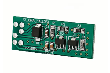
Soldering Techniques for Different Component Packages in PCB Assembly
PCB assembly involves a wide range of component packages, each requiring specific soldering approaches to ensure reliability and performance. Understanding the nuances of handling surface-mount devices (SMDs), through-hole components, and specialized packages like ball grid arrays (BGAs) is critical for minimizing defects and optimizing production yields.
Surface-Mount Devices (SMDs): Precision in Placement and Reflow
SMDs, including resistors, capacitors, and integrated circuits (ICs), dominate modern PCB designs due to their compact size and automation compatibility. Successful soldering begins with accurate placement using pick-and-place machines or manual tweezers for prototypes. Misalignment during placement can lead to open circuits, shorts, or tombstoning, where one terminal lifts off the pad during reflow.
Reflow soldering is the primary method for attaching SMDs. The process involves applying solder paste to pads, placing components, and heating the board through a controlled temperature profile. Key considerations include paste viscosity, stencil thickness, and aperture design to ensure consistent solder deposition. For fine-pitch components, laser-cut stainless-steel stencils with electroformed apertures improve paste release accuracy, reducing bridging or insufficient solder.
During reflow, ramp rates and peak temperatures must align with component and solder alloy specifications. Lead-free solders, commonly used today, require higher reflow temperatures than traditional tin-lead alloys, increasing the risk of thermal damage to sensitive components. Nitrogen atmospheres in reflow ovens minimize oxidation, improving wetting and reducing voiding in joints. Post-reflow inspection using automated optical inspection (AOI) or X-ray systems helps identify defects like head-in-pillow or misaligned BGAs early in production.
Through-Hole Components: Managing Heat and Mechanical Stress
Through-hole components, such as connectors, electrolytic capacitors, and transformers, remain essential for applications requiring high mechanical strength or high current capacity. Unlike SMDs, these parts are inserted into drilled holes and soldered to pads on both sides of the PCB. Wave soldering and selective soldering are the two primary methods for attaching through-hole components, each with distinct advantages.
Wave soldering involves passing the PCB over a molten solder wave, which wets exposed leads and pads. Fixturing is critical to protect SMDs from the solder wave and ensure consistent joint formation. Flux application, preheat temperatures, and conveyor speed must be optimized to prevent solder splatter, icicles, or cold joints. For mixed-technology boards (combining SMDs and through-hole parts), selective soldering offers greater control by using miniature solder nozzles to target specific areas, reducing thermal stress on adjacent components.
Manual soldering remains viable for low-volume production or rework. Temperature-controlled soldering irons with fine tips enable precise heat delivery to joints without overheating the PCB or component bodies. Using the correct solder wire diameter and flux type ensures proper wetting and minimizes dross formation. For high-reliability applications, inspecting joints for fillet shape, voids, and excess solder is essential to confirm mechanical and electrical integrity.
Ball Grid Arrays (BGAs) and Fine-Pitch Packages: Mitigating Voiding and Alignment Challenges
BGAs and other fine-pitch packages, such as chip-scale packages (CSPs) and quad-flat no-leads (QFNs), pose unique challenges due to their small pitch sizes and hidden solder joints. BGAs feature an array of solder balls on their underside, which reflow onto corresponding pads on the PCB. Achieving reliable connections requires meticulous control of reflow parameters, including soak time, reflow temperature, and cooling rate.
Voiding in BGA joints is a common issue caused by trapped flux residues or outgassing during reflow. Reducing voiding involves optimizing paste formulation, using vacuum reflow ovens to remove air during melting, or implementing underfill materials post-assembly to enhance mechanical stability. X-ray inspection is indispensable for detecting voids, misaligned balls, or bridging beneath the package, as these defects are invisible to optical inspection.
For QFNs and similar packages, managing the thermal pad in the center of the component is crucial. This pad connects to a large copper area on the PCB for heat dissipation but can trap air if not properly vented. Designing thermal vias in the pad area improves solder flow and reduces the risk of voiding. During assembly, ensuring the component is flat against the PCB before reflow prevents uneven solder distribution, which could lead to open circuits or warping under thermal cycling.
Handling Specialized Packages: Flexibility and Adaptability
Beyond standard packages, PCB assembly may involve specialized components like leaded ceramic chip carriers (LCCCs), plastic leaded chip carriers (PLCCs), or multi-chip modules (MCMs). Each requires tailored approaches based on their physical and thermal properties. For example, LCCCs with gold-plated leads demand compatible flux types to prevent corrosion, while MCMs with stacked dies may require localized heating to avoid damaging lower layers during rework.
Flexibility in tooling and process parameters is essential when working with diverse packages. Adjustable nozzle sizes in selective soldering systems, custom stencils for paste application, and modular fixturing accommodate varying component heights and footprints. Training operators to recognize package-specific defects, such as lifted leads on PLCCs or cracked solder balls on BGAs, ensures quick corrective actions during production.
By mastering these techniques—from SMD placement to BGA inspection—manufacturers can address the complexities of modern PCB assembly, delivering high-quality products across industries ranging from consumer electronics to aerospace.


