Electrical Performance Requirements for PCB Manufacturing in Electric Vehicle Charging Stations
Electric vehicle (EV) charging stations demand PCBs engineered to handle high power, rapid switching frequencies, and complex communication protocols while ensuring safety and reliability under diverse environmental conditions. These systems must balance efficient power conversion, electromagnetic compatibility (EMC), and thermal stability to meet international standards and user expectations. This article explores the critical electrical performance requirements for PCBs in EV charging stations, focusing on high-voltage and high-current handling, signal integrity for communication interfaces, and robust insulation and safety features.
High-Voltage and High-Current Handling for Power Conversion Modules
EV charging stations operate at voltage levels ranging from 240V AC in residential chargers to 1000V DC in fast-charging systems, requiring PCBs capable of managing extreme electrical stress without arcing or insulation failure. High-voltage PCBs must incorporate wide creepage and clearance distances between conductive traces to prevent electrical discharge. Creepage distances—the shortest path along a surface between two conductors—are extended using raised barriers, conformal coatings, or slot isolation to meet safety standards like IEC 61851 for EV charging equipment. Clearance distances, the air gap between conductors, are optimized through precise layer stacking and via placement to avoid voltage breakdown, especially in humid or dusty environments.
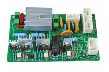
For high-current applications, such as DC fast chargers delivering over 350kW, PCBs use thick copper traces (typically 3–10 oz/ft²) to minimize I²R losses and reduce heat generation. Embedded copper busbars or heavy copper layers are integrated into the PCB substrate to carry currents exceeding 500A without excessive voltage drops. These designs eliminate the need for external wiring, improving reliability and simplifying assembly. Manufacturers also employ partial discharge (PD) testing during production to detect insulation weaknesses in high-voltage zones, ensuring long-term durability under continuous operation.
Power electronics in charging stations, including IGBTs (Insulated Gate Bipolar Transistors) and MOSFETs, generate rapid switching transients that can induce voltage spikes or electromagnetic interference (EMI). PCBs must incorporate decoupling capacitors and snubber circuits placed close to switching devices to suppress noise and stabilize voltage levels. Additionally, manufacturers use laminated busbars with optimized geometries to reduce parasitic inductance, preventing voltage overshoot during high-frequency switching.
Signal Integrity and Communication Protocol Compliance for Control Systems
Modern EV charging stations rely on multiple communication protocols—such as CAN (Controller Area Network), PLC (Power Line Communication), and Ethernet—to coordinate power delivery, user authentication, and billing. PCBs must maintain signal integrity across these interfaces to prevent data errors or system malfunctions. For high-speed communication (e.g., 100Mbps Ethernet), PCBs use controlled impedance traces with precise width and spacing to match the characteristic impedance of the cable, minimizing reflections and signal attenuation. Differential pair routing is employed for protocols like CAN and RS-485 to reject common-mode noise from power electronics or external EMI sources.
EMI shielding is critical in charging station PCBs to prevent interference between power and communication circuits. Manufacturers integrate grounded copper planes or shielding layers into the PCB stackup to isolate sensitive analog and digital signals from high-voltage switching noise. For outdoor installations, conformal coatings with EMI-absorbing properties may be applied to further reduce radiated emissions. Additionally, PCBs for communication modules adhere to standards like ISO 15118 for vehicle-to-grid (V2G) communication, ensuring compatibility with diverse EV models and charging networks.
Timing accuracy is another requirement for control systems in charging stations, particularly for synchronization between power conversion and billing cycles. PCBs use low-skew clock distribution networks and high-precision oscillators to ensure synchronous operation across multiple microcontrollers or FPGAs. For example, in DC fast chargers, precise timing coordination between battery management system (BMS) communication and power delivery is essential to prevent overcharging or thermal runaway in connected vehicles.
Insulation and Safety Features for User and Equipment Protection
Safety is paramount in EV charging station PCBs, which must comply with standards like UL 2202 and IEC 62955 to protect users from electric shock and equipment from fire hazards. High-voltage PCBs incorporate double insulation or reinforced insulation between live parts and accessible surfaces, using materials with high dielectric strength (e.g., polyimide or FR-4 with high-Tg ratings). Insulation resistance testing is performed during manufacturing to verify that leakage currents remain below 0.5mA, even under潮湿 or contaminated conditions.
Thermal isolation is another safety feature in charging station PCBs, particularly for components like fuses or relays that generate heat during fault conditions. Manufacturers use thermally conductive but electrically insulating materials (e.g., ceramic-filled epoxy) to transfer heat away from hotspots while maintaining electrical isolation. For example, PCBs may include embedded thermal pads beneath power semiconductors to prevent localized overheating that could degrade insulation or trigger false trips in protective devices.
Fault tolerance is built into PCB designs through redundant current paths and self-diagnostic capabilities. For instance, PCBs for AC chargers may include dual current sensors to detect imbalances between live and neutral wires, triggering a shutdown if a ground fault is detected. Similarly, DC fast chargers use isolated gate drivers for power semiconductors to ensure safe operation even if one control channel fails. Manufacturers also incorporate arc-resistant coatings on PCB surfaces to prevent tracking or carbonization during electrical faults, enhancing safety in high-voltage applications.
As EV adoption accelerates, PCB manufacturers must continuously innovate to meet the evolving electrical performance demands of charging stations. By prioritizing high-voltage/current handling, signal integrity, and safety features, the industry can produce PCBs that enable efficient, reliable, and user-friendly charging infrastructure for the next generation of electric vehicles.