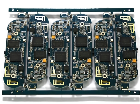
Technical Advantages
High Density Interconnect (HDI): Provides advanced circuit density through microvias and buried vias for compact design without compromising performance.
12-layer stack-up: Provides ample layers for complex routing, ensuring high-speed signal integrity and efficient power delivery.
High-speed signal transmission: Optimized for minimal signal loss and impedance matching, ideal for high-bandwidth applications.
Heat dissipation: Thermal vias and advanced materials are used to maintain stable operating temperature during intensive use.
Rugged manufacturing: Manufactured with high-reliability materials and manufacturing processes to ensure durability and long-term performance.
Industry-compliant: Manufactured in accordance with IPC and UL standards to ensure safety and quality.
Technical specifications
| Parameter | Specifications |
| Frequency Range | Up to 20 GHz |
| Number of Layers | 12 layers |
| Minimum Trace Width/Spacing | 3 mil (0.075 mm)/3 mil (0.075 mm) |
| Microvia Diameter | 0.1 mm |
| Material | High-speed, low-loss dielectric |
| Operating Temperature | -40°C to 125°C |
| Surface Finish | ENIG (Electroless Nickel Immersion Gold) |
| Compliance | IPC-6012 compliant, UL 94V-0 rated |
Applications
1.Tablets: Designed for high-performance tablets that require fast data processing and high-speed connectivity.
2.Smartphones: For advanced smartphones with demanding processing needs.
3.High-performance computing devices: Ideal for devices that require dense circuits and high-speed signal transmission.
4.Embedded systems: Enhance the performance of systems that require compact, high-density PCBs.
5.IoT Devices: Support IoT devices with complex circuit requirements.
PCB Services
Tailor-made solutions to meet customer-specific requirements for layer count, trace width, and signal routing.
Fast turnaround HDI PCB prototypes to accelerate development cycles.
Scalable manufacturing to meet mass production needs with consistent quality.
End-to-end solutions including component sourcing, assembly, and testing.
Comprehensive testing services to ensure compliance with industry standards and customer specifications.


