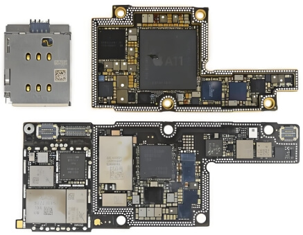
Our Product Benefits
Excellent Signal Integrity:Minimizes signal loss and improves data transmission quality, ensuring clear communications.
Advanced Thermal Management:Uses cutting-edge heat dissipation technology to maintain optimal operating temperature even at high-frequency operation.
Rugged Manufacturing:Designed with durability in mind, our PCBs withstand the rigors of daily use, ensuring long-term reliability and performance.
Industry Compliant:Manufactured to RoHS and IPC standards, ensuring a safe environment and compliance with global regulations.
Product Specifications
| Parameter | Specifications |
| Frequency Range | Supports 5G mmWave bands (24 GHz – 90 GHz) |
| Number of Layers | Up to 10 layers |
| Minimum Trace Width/Spacing | 3 mil (0.075 mm) |
| Via Diameter | 0.1 mm |
| Material | High-frequency, low-loss dielectric |
| Operating Temperature | -40°C to 125°C |
| Compliance | RoHS compliant, IPC-7351 certified |
Assembly Process
1.Design
Utilizes advanced software for precise layout and design, ensuring minimal interference and optimal signal routing.
2.Manufacturing:
2.1Etching: High-precision etching to accurately define circuit paths.
2.2Drilling: State-of-the-art through-hole drilling to ensure inter-layer connectivity.
2.3Lamination: Carefully layering materials to maintain structural integrity and signal consistency.
3.Component Assembly:
3.1Surface Mount Technology (SMT): High-speed, high-precision placement of components.
3.2Through-Hole Technology (THT): Robust mounting of components that require greater mechanical strength.
3.3Hybrid Technology: Integrate SMT and THT components to meet a variety of application needs.
4.Testing and Inspection:
4.1Automated Optical Inspection (AOI): Ensure component placement accuracy.
4.2In-Circuit Test (ICT): Verify electrical connections and functionality.
4.3Functional Testing: Comprehensive testing to ensure performance under real-world conditions.
Our Services
Custom PCB Design: Tailored to specific customer requirements to ensure your vision is realized.
Rapid Prototyping: Rapidly complete prototyping to accelerate product development.
Mass Production: Scalable manufacturing to meet the needs of high-volume production.
PCB Assembly: Provide SMT, THT, and Hybrid Technology assembly services with strict quality control.
Testing and Validation: Extensive testing to ensure compliance with industry standards and customer specifications.


