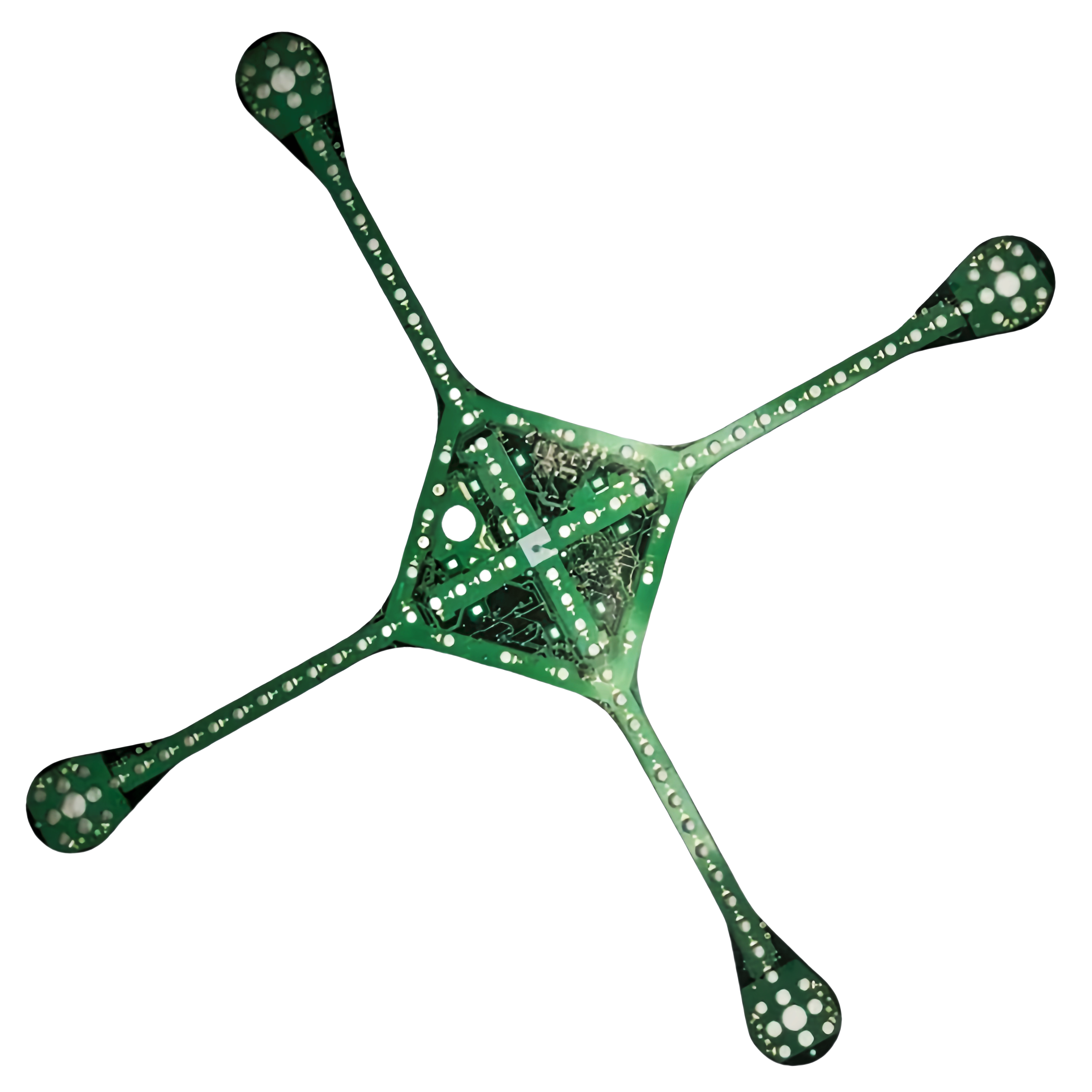
Drones usually use 6-layer PCB design to meet the functional requirements of the equipment. 6 layers means that there are 6 conductive patterns on the inside and outside of the circuit board, which can effectively increase the connection density of the circuit and reduce the wiring length per unit area.
Immersion gold surface treatment process,
Immersion gold is a surface treatment process that usually forms a thin layer of gold on the pads and contact points of the PCB to improve welding performance and anti-oxidation ability. Immersion gold treatment can provide better electrical connection and longer service life.
The immersion gold surface can effectively prevent oxidation and wear, ensure the connection stability in long-term use, and is particularly suitable for high-frequency and high-speed applications.
The good conductivity and wettability of the metal pad make the welding process smoother, especially suitable for the welding of SMT (surface mount technology) components.
FR-4 material and immersion gold surface treatment can effectively reduce signal loss, improve the electrical performance of the PCB, and are suitable for high-frequency applications.
Use PCB design software to complete the circuit diagram and layout, ensure that the double-sided circuit wiring is reasonable, and the signal
Make FR-4 substrate according to the design file, clean and dry it, and prepare for subsequent processing.
Etch the substrate surface to form the required circuit pattern, and then cover it with a thick layer of copper to ensure conductivity.
Generate a gold layer on the pads and contact points through chemical deposition, complete the gold treatment, and ensure good conductivity and oxidation resistance in the welding area.
Conduct electrical tests and quality inspections to ensure that the PCB meets standard requirements before leaving the factory.


