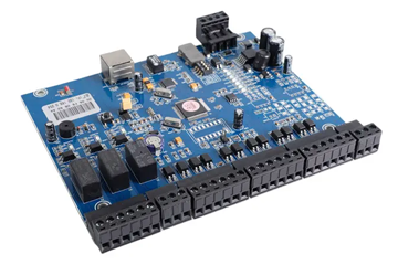
Quality Inspection Methods for Solder Joints in PCB Assembly: Ensuring Electrical and Mechanical Reliability
Solder joints are critical to PCB functionality, serving as electrical connections and mechanical anchors for components. Defects like cold joints, voids, or bridging can lead to intermittent failures or complete device malfunction. Effective inspection methods are essential to identify these issues early in production. Below are key techniques for evaluating solder joint quality, covering visual, microscopic, and non-destructive approaches.
Visual Inspection: Basic Yet Essential for Surface-Level Defects
Visual inspection is the first line of defense in solder joint quality control, relying on trained operators or automated systems to identify obvious defects. This method involves examining solder joints under magnification, typically 10x–20x, to check for irregularities such as insufficient solder (dry joints), excess solder (solder balls or bridges), or misaligned components. Proper lighting is crucial to highlight surface textures and contrasts, enabling detection of cracks or poor wetting, where solder fails to adhere smoothly to pads or leads.
Key visual indicators of quality include a smooth, concave fillet shape, which indicates proper solder flow and adhesion. A convex or irregular fillet may signal insufficient heat during reflow or contamination on the pad surface. Component leads should be centered on pads with no visible gaps, as misalignment can create stress points during thermal cycling or mechanical vibration. While visual inspection is quick and cost-effective, it is limited to surface-level defects and cannot detect internal voids or subsurface cracks.
X-Ray Inspection: Revealing Hidden Defects in Complex Assemblies
X-ray imaging is indispensable for inspecting solder joints in dense or multi-layer PCBs, where visual access is obstructed by components or the board itself. This non-destructive technique penetrates materials, allowing inspection of internal structures like ball grid arrays (BGAs), quad flat no-leads (QFNs), or through-hole vias. X-rays highlight voids—air pockets trapped within solder joints—which can reduce mechanical strength and thermal conductivity, leading to premature failure under stress.
The percentage of voids is a critical metric; industry standards often specify thresholds (e.g., less than 25% voiding in BGA joints) to ensure reliability. X-ray systems also detect bridging between adjacent pins or pads, which may not be visible externally but can cause short circuits. Advanced systems use computed tomography (CT) to generate 3D models of solder joints, enabling detailed analysis of volume, shape, and alignment. However, X-ray inspection requires specialized equipment and trained personnel to interpret images accurately, making it more suitable for high-value or safety-critical applications.
Electrical Testing: Verifying Functionality Through Continuity and Isolation Checks
Electrical testing confirms that solder joints provide reliable electrical connections without unintended pathways. Continuity testing checks for open circuits by applying a low-voltage current between connected points, such as a component lead and its corresponding pad. A lack of continuity indicates a defective joint, often caused by insufficient solder or a cracked connection. Isolation testing, conversely, ensures no shorts exist between adjacent traces or pads by measuring resistance; values below a specified threshold signal bridging or contamination.
In-circuit testing (ICT) and flying probe testing are common electrical methods for high-volume production. ICT uses custom fixtures with probes to contact test points simultaneously, offering fast, comprehensive coverage but requiring upfront fixture design costs. Flying probe testers, equipped with movable probes, are more flexible for low-volume or prototype assemblies, though slower due to sequential testing. Electrical testing is often combined with other methods, as it confirms functionality but cannot identify mechanical defects like weak joints or voids that may not yet affect conductivity.
Microscopic Analysis: High-Resolution Examination of Joint Integrity
Microscopic inspection provides detailed analysis of solder joint microstructure, revealing defects invisible to the naked eye or standard magnification. Scanning electron microscopy (SEM) offers high-resolution imaging (up to nanometer scale) to detect intermetallic compound (IMC) layer thickness, which influences joint durability. A thin, uniform IMC layer indicates proper soldering, while excessive growth can make joints brittle. SEM also identifies micro-cracks or delamination at the solder-pad interface, which may propagate under thermal or mechanical stress.
Optical microscopy, while lower in resolution than SEM, is more accessible for routine inspection. It examines joint surface finish, wetting angles, and the presence of flux residues, which can corrode joints over time if not cleaned properly. Cross-sectional analysis involves cutting a solder joint and polishing it for microscopic examination, providing insights into internal void distribution or layer separation. This destructive method is typically reserved for failure analysis or research rather than production-line testing.
Thermal Cycling and Mechanical Testing: Simulating Real-World Stress Conditions
To validate long-term reliability, solder joints undergo accelerated life testing that mimics operational stressors like temperature fluctuations and mechanical vibration. Thermal cycling subjects PCBs to repeated heating and cooling between extreme temperatures (e.g., -40°C to 125°C), causing materials to expand and contract. Joints with voids or weak IMC layers are more likely to crack under this stress, leading to electrical failure. Monitoring resistance changes during cycling helps predict joint lifespan.
Mechanical testing evaluates joint strength under physical force, such as pull or shear tests. These tests measure the force required to detach a component lead from its pad, with higher values indicating better adhesion. For surface-mount devices (SMDs), shear testing assesses the bond between the solder and component terminal, while pull testing evaluates the entire joint’s integrity. Data from these tests inform design decisions, such as pad geometry or solder alloy selection, to enhance durability in high-vibration environments like automotive or aerospace applications.
By integrating visual, X-ray, electrical, microscopic, and stress testing methods, manufacturers can comprehensively evaluate solder joint quality. Each technique addresses specific defect types, ensuring defects are detected and resolved before products reach end-users, thereby enhancing reliability and reducing field failures.


