Detailed explanation of the PCBA processing flow of smart door pins: 8 core steps from prototype to mass production
As an important part of smart home, the performance and quality of smart door pins directly affect user experience and safety. PCBA (printed circuit board assembly) processing is a key link in the manufacturing of smart door pins, covering multiple steps from circuit board design to finished product testing. This article will introduce the 8 core steps in the PCBA processing flow of smart door pins in detail, and introduce the professional capabilities and services of XDCPCBA PCB assembly factory in this field.

1. Demand analysis and communication
The first step in the PCBA processing of smart door pins is to conduct demand analysis and communication. XDCPCBA PCB assembly factory has in-depth exchanges with customers to clarify detailed requirements such as circuit board size, number of layers, materials, component types and quantity, and welding methods. At the same time, the two parties reached a consensus on key indicators such as product functions, performance, and cost to ensure that subsequent design and production can accurately meet customer needs. At this stage, the professional team of the electronic contract manufacturer (EMS) will sign a detailed cooperation agreement with the customer to ensure the rights and interests of both parties.
2. Circuit design
After clarifying the customer's needs, XDCPCBA's design team will use professional electronic design automation (EDA) software to design and draw the circuit schematic. The designer fully considers the reliability, stability and manufacturability of the circuit to ensure that the design scheme not only meets the product performance requirements, but also facilitates subsequent patch processing and assembly. The Gerber files and drilling files generated at this stage will be used in the subsequent circuit board manufacturing process.

3. PCB production
After the circuit design is completed, the PCB (printed circuit board) production stage will begin. As a professional 2-30 layer PCB manufacturer, XDCPCBA has advanced PCB production lines and process technologies. PCB production includes multiple complex processes such as board cutting, drilling, electroplating, and circuit printing. During the production process, XDCPCBA strictly controls various process parameters to ensure the quality and accuracy of the PCB. For complex structures such as multi-layer boards or high-density boards, XDCPCBA uses advanced lamination technology and precise alignment systems to ensure precise alignment and electrical connections between layers. In addition, XDCPCBA also provides 2-6 layer PCB free proofing services to help customers verify designs and reduce upfront costs.
4. Component procurement and inspection
While PCB is being made, XDCPCBA's procurement department will purchase components according to the BOM list (component list) determined in the circuit design plan. XDCPCBA has established long-term cooperative relationships with world-renowned component suppliers to ensure that the quality and performance of the purchased components meet the requirements. Before the components are put into storage, XDCPCBA conducts strict quality inspections, including appearance inspection, performance testing, reliability evaluation and other links to ensure that only components that meet the standards can be used for subsequent patch processing.

5. SMT patch processing
After the components are purchased, they enter the SMT (surface mount technology) patch processing stage. XDCPCBA has a number of advanced SMT production lines that can efficiently and accurately complete the placement of components. During the patch processing process, XDCPCBA uses an automatic patch machine to accurately place surface mount components (such as resistors, capacitors, ICs, etc.) on PCB pads printed with solder paste. The patch machine achieves precise placement by identifying the packaging form of the components and the markings on the PCB. Subsequently, the components are firmly connected to the PCB through the reflow soldering process.
6. Plug-in processing and wave soldering
For components that cannot be processed by the SMT machine (such as large connectors, heat sinks, etc.), XDCPCBA will perform manual plug-in. After the plug-in is completed, it enters the wave soldering stage. Wave soldering is to pass the PCB with the components inserted through the wave soldering machine, and use the wave-shaped solder to flow through the solder joints of the PCB to achieve welding. Wave soldering is suitable for the welding of pin components, and has the advantages of fast welding speed, high efficiency and low cost. After the welding is completed, XDCPCBA will also perform foot cutting and post-welding processing to ensure the welding quality.
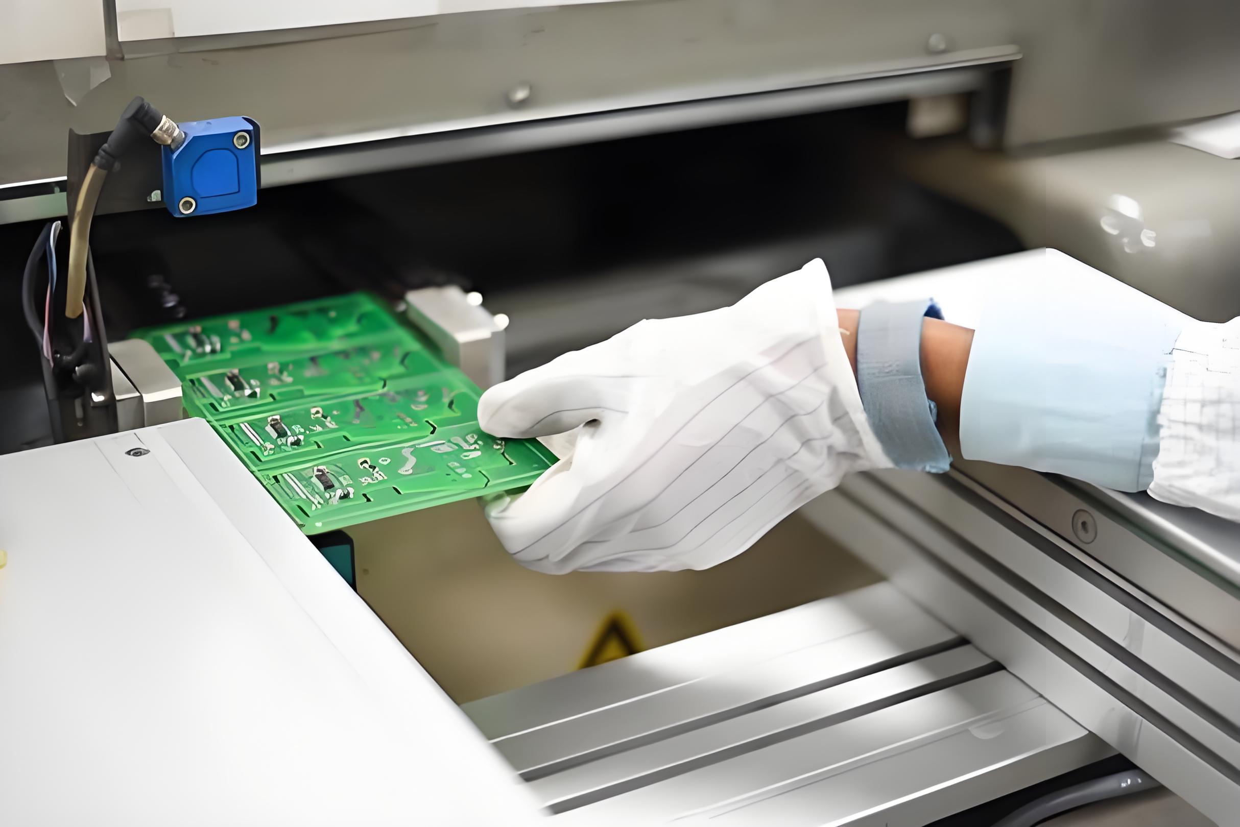
7. Quality inspection and functional testing
After the welding is completed, XDCPCBA will conduct strict quality inspection and functional testing. Quality inspection includes multiple links such as appearance inspection and welding quality inspection to ensure that the PCBA is free of defects such as damage, deformation, and pollution. Functional testing uses professional testing instruments to test the electrical performance and function of the PCBA to ensure that it meets the design requirements. XDCPCBA also uses automatic optical inspection (AOI) equipment to perform online inspection of welding quality to detect and solve welding defects in time.

8. Finished product assembly, testing and delivery
After passing the quality inspection and functional test, XDCPCBA will assemble the finished product. The assembly process includes steps such as installing the housing and connecting the power supply. After the assembly is completed, the final test is carried out to verify the overall function and performance of the product. The test content includes electrical performance test, functional performance test, environmental adaptability test, reliability test, etc. The products that pass the test will be cleaned, packaged, labeled, and protected against static electricity and moisture. Finally, XDCPCBA will ship according to customer requirements, provide shipping documents and necessary technical documents to ensure that customers receive the goods in time.
As a professional PCBA processing plant and electronic contract manufacturer, XDCPCBA PCB assembly factory has rich experience and advanced technology in the field of smart door pin PCBA processing. From prototype to mass production, XDCPCBA always adheres to customer demand-oriented, strictly controls every processing link, and ensures the performance and reliability of the final product. Whether it is 2-6 layer PCB free proofing service, or efficient SMT PCB assembly and wave soldering process, XDCPCBA can provide customers with a full range of PCBA processing solutions.


