PCB (Printed Circuit Board) manufacturing process flow is a complex and sophisticated process, involving multiple steps and links. The following is an introduction to the main process flow of PCB manufacturing:
First, the design stage
Circuit schematic design
Steps: electronic engineers according to the functional requirements of electronic products, the use of professional circuit design software (such as Altium Designer, OrCAD, Cadence Allegro, etc.) to draw circuit schematics.
Content: Define the electrical connection relationship of each electronic component in the schematic diagram, including the selection and layout of components such as resistors, capacitors, chips, inductors, etc., and determine key information such as signal flow direction and power distribution.
Purpose: To ensure that the circuit can realize the expected functions, such as signal amplification, filtering, data processing and so on.
PCB layout and wiring design
Steps: Place the electronic components in the schematic on the physical space of the PCB and plan the electrical connection lines between the components.
Considerations: Functional grouping of components, signal transmission paths, heat dissipation requirements, mechanical structure, mounting methods (e.g., surface mount SMT or plug-in mounting) and so on.
Purpose: Ensure that the layout facilitates subsequent manufacturing while ensuring signal integrity and electrical performance.
Design Rule Check (DRC)
Steps: Use DRC software to conduct a comprehensive check of the design file.
Check content: including line width, line spacing, via size, pad size and other parameters are compliant.
Purpose: To ensure that the design scheme can be smoothly transformed into actual products.
Output Gerber file
Step: Convert the designed PCB file to Gerber file.
Content: Gerber file is a commonly used data transfer format in the PCB manufacturing industry, which contains graphical information about the various layers of the PCB board (e.g. top layer, bottom layer, inner layer, etc.).
Purpose: To facilitate the production of PCB manufacturers.
Second, the preparation stage
Substrate material selection
Materials: Common substrate materials include FR-4 (glass fiber reinforced epoxy resin), polyimide (PI), polytetrafluoroethylene (PTFE), and so on.
Considerations: Select the appropriate substrate material based on the PCB application scenario and performance requirements. For example, FR-4 substrates are widely used because of their low cost and stable performance; polyimide substrates are suitable for electronic products that require flexibility.
Purpose: To ensure the mechanical strength, electrical conductivity and thermal stability of the circuit board.
Copper Foil Preparation
Material: Copper foil is the main material used for conductivity in PCBs, usually electrolytic copper foil or calendered copper foil.
Selection basis: According to the design requirements of PCB, select the appropriate thickness and purity of copper foil. High purity copper foil has better conductivity.
Purpose: To ensure the conductivity of the circuit board.
Preparation of other materials
Materials: including solder resist ink, screen printing ink, surface treatment materials (such as gold immersion, tin plating, organic solder-protection film OSP, etc.), dry film, ink, chemical potions (etching solution, plating solution, etc.), drilling pins and other auxiliary materials.
Purpose: to meet the PCB manufacturing process in a variety of process requirements.
Third, the manufacturing stage
Cutting
Steps: the use of cutting equipment (such as CNC cutting machine) will be large-size substrate materials in accordance with the PCB design dimensions for cutting, to get the required board.
Requirements: Ensure that the size is accurate and the edges are flat.
Inner layer production
Steps:
Pre-treatment: Surface cleaning and roughening of the open copper-clad board to increase the adhesion of the dry film to the surface of the board during subsequent film pressing.
Lamination: Laminating the dry film (a light-sensitive polymer film) onto the surface of the treated copper-clad laminates by hot pressing.
Exposure: The laminate is placed under an exposure machine and the dry film is exposed by UV light according to the inner circuit pattern in the Gerber file.
Developing: The unexposed dry film is dissolved and removed using a developing solution, leaving the exposed dry film pattern.
Etching: Remove the unwanted copper foil using etching solution to form the inner layer line.
De-filming: Remove the residual dry film on the inner layer line by chemical solution or mechanical means.
Browning treatment: brown the inner layer of the circuit board, so that the inner layer of the line surface to form a uniform layer of oxide film, enhance the adhesion with the semi-cured sheet.
Lamination
Steps: Stack the multilayer inner layer circuit boards with the semi-cured sheet (a kind of glass fiber cloth pre-impregnated with resin) in a certain order, and use a vacuum laminating machine to press the laminated boards together.
Purpose: Firmly bond the layers together to form a multilayer PCB board.
Requirements: Precise control of temperature, pressure, time and other parameters to prevent bubbles, delamination and other defects.
Drilling
Steps: According to the PCB design, use CNC drilling machine to drill various apertures of over-holes and mounting holes.
Purpose: To realize the electrical connection between different layers and component installation.
Requirements: Control the drilling speed, feed and other parameters to ensure that the hole wall is smooth and the hole position is accurate.
Hole metallization and plating
Steps:
Hole Metallization: Activate the hole wall, then deposit a layer of conductive material (e.g. copper) on the hole wall to realize the metallization of the hole wall.
Plating: Plating of the entire PCB board, thickening the copper layer to meet the line conductive and mechanical strength requirements.
Purpose: To ensure that the PCB can transmit current between layers.
Outer Layer Fabrication
Steps: similar to the production of the inner layer, including the outer layer of film, exposure, development, etching, de-filming and other steps to form a complete outer layer of the line.
Purpose: To complete the visible circuit connections on the PCB board.
Soldermask production
Steps: Coated with soldermask ink on the PCB board surface, through the exposure, development and other processes, so that the need to weld the components of the pad area exposed, the rest of the area is covered by ink.
Purpose: To prevent short-circuiting during the soldering process, and at the same time protect the lines from external environmental erosion.
Character Printing
Steps: The use of screen printing or inkjet printing and other technologies, PCB board surface printing component identification, model, version number and other character information.
Purpose: To facilitate subsequent assembly and maintenance.
Surface treatment
Steps: Select the appropriate surface treatment process according to product requirements, such as gold sinking, tin spraying, OSP and so on.
Purpose: Improve the solderability and oxidation resistance of PCB.
Fourth, testing and packaging stage
Appearance Inspection
Steps: Through manual visual inspection or automatic optical inspection (AOI) equipment to check the appearance of the PCB.
Inspection content: to see whether there are line defects (such as broken circuit, short circuit), copper foil warping, bad pads, etc., as well as soldermask layer, whether the character printing is complete and clear.
Purpose: To ensure that the appearance of the PCB quality meets the requirements.
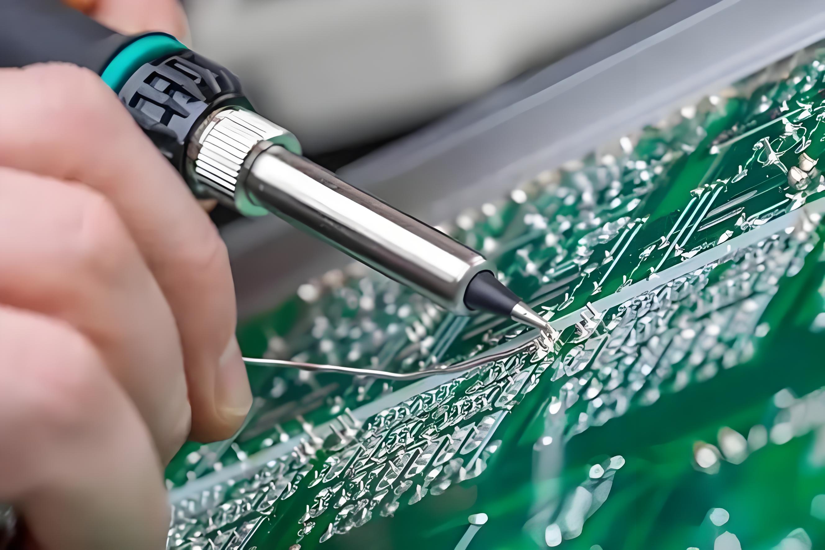
Electrical performance test
Steps: Use professional test equipment (such as flying probe tester, ICT tester, etc.) to test the electrical performance of the PCB.
Test content: including circuit conductivity, insulation resistance, impedance matching and other parameters.
Purpose: To verify whether the line meets the design requirements and to ensure that the electrical performance of the PCB is stable and reliable.
Reliability Test
Steps: Reliability testing according to product requirements, such as high-temperature aging test, cold and hot shock test, vibration test, etc..
Purpose: To ensure that the PCB can work stably for a long time under various complex environments.
Packing and Shipping
Steps: Pack the qualified PCBs, and then ship them out according to customer requirements.
Packaging: Usually use anti-static bag, upper and lower tape, release film, etc..
Purpose: to protect the PCB from damage during transportation.
Fifth, attention
Quality control: In the whole production process, quality control is a crucial part. It is necessary to establish a strict quality management system to strictly control each link to ensure the quality and performance of the final product.
Continuous Improvement: By collecting customer feedback and market information, the production process is continuously improved and optimized to increase product competitiveness and market share.
The PCB manufacturing process is a complex and precise process involving multiple steps and links. Only by precisely controlling the process parameters and quality requirements of each link can we ensure the production of high quality PCB products.
Translated with DeepL.com (free version)


