In the PCB(printed circuit board) assembly process, DFM(Design for Manufacturing, design for manufacturing) design rule inspection is a key link to ensure that PCB design meets manufacturing process requirements, improve production efficiency and reduce costs. The following is a detailed summary of the inspection of DFM design rules in the PCB assembly process:
First, the importance of DFM design rule check
DFM design rule inspection is the process of conducting a comprehensive review of the design document after the PCB design is completed, aiming to find and solve the problems existing in the design and ensure the manufacturability of the PCB. Through DFM design rule inspection, it can reduce the rework rate in the production process, improve the production efficiency and product quality, and reduce the production cost.
Second, the main content of DFM design rule check
Component layout check
Component spacing rationality: Check whether the spacing between the components on the PCB is sufficient to avoid solder bridging or short circuit during welding. In general, for surface mount technology (SMT) components, the pin spacing should be kept within a reasonable range, such as 0.5mm or more.
Large-size component layout: Check whether the layout of large-size components (such as power modules, large electrolytic capacitors, etc.) is reasonable, and avoid the layout of the PCB edge or weak areas near the edge of the board to enhance the structural stability of the PCB.
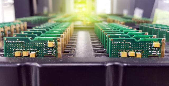
Component direction consistency: try to design the same type of components in the same direction, so that the machine can install components in one direction during production and improve production efficiency.
Wiring check
Line width and line distance: Check whether the line width meets the production process requirements, too thin line width may appear in the etching process break the risk, and too wide line width will waste PCB space. At the same time, the line spacing should also be sufficient to prevent short circuits between adjacent lines. In general, for ordinary FR4 material PCB, the line width and line distance between 0.15mm and 0.2mm are more common.
Signal integrity: Check the length, direction and number of holes of high-speed signal lines to ensure that the signal does not distort during transmission. Signal lines should be as short and straight as possible to avoid excessive bending and holes. For key high-speed signals, such as clock signals and differential signals, strict impedance matching design should be carried out.
Pad design check
Pad size matching: Check that the size of the pad matches the size of the component pin to avoid weak welding or pins that cannot fit into the pad.
Correct pad shape: according to the shape of the component pin and the actual need to choose the appropriate pad shape, such as round, square, oval, etc.
Solder stop treatment: Check whether the solder stop treatment is done around the pad to avoid green oil (solder stop layer) covering the pad and affecting the welding.
Hole design check
Aperture and hole distance: Check whether the diameter and position of the drilling hole meet the manufacturing requirements to avoid manufacturing difficulties caused by too small aperture or inaccurate position. At the same time, check whether the hole distance meets the requirements to prevent problems such as drill break or short circuit in the drilling process.
Hole ring size: Check whether the hole ring size is enough to avoid the weak adhesion of the hole disk resulting in the welding or maintenance of the pad.
Special process requirements check
Blind burials, HDI, etc. : If the PCB design contains special processes, such as blind burials, HDI(high-density interconnect), etc., check whether these special processes match the process capabilities of the manufacturer.
Rigid and flexible plate: For rigid and flexible plate, it is necessary to check whether the special flexible materials and pressing process required for its production are met.
Testability design check
Test point Settings: Check whether enough test points are set and whether the location of the test point is convenient for the contact of the test equipment. For some complex PCBS, you should also consider whether you need to design a test interface such as boundary scan test (JTAG).
Test point layout: The layout of test points should follow certain rules, such as evenly distributed on the PCB surface, avoid being blocked by components, and maintain a certain distance from adjacent components.
Other examination
PCB material selection: Check whether the selected PCB material is suitable for the production process and the application environment of the product, to avoid PCB deformation, delamination or electrical performance degradation due to material problems in the production process.
Process edge and positioning hole: Check whether the edge of the PCB board is set aside a sufficient width of the process edge, so that the machine can grip the board for processing during production. At the same time, check whether enough positioning holes are designed to ensure the accuracy of component installation and welding.
Third, the implementation of DFM design rule inspection
DFM design rule checks can be carried out by professional DFM check software or tools, which usually have a set of predefined design rules that the designer can customize or use to check the manufacturability of the design. During the inspection process, the software will automatically mark all the places that do not meet the rules, and the designer can modify and optimize according to the prompts.
Fourth, summary
DFM design rule inspection is an indispensable part of the PCB assembly process, through comprehensive inspection and optimization, you can ensure the manufacturability of PCB design, improve production efficiency and product quality, and reduce production costs. Therefore, in the PCB design process, full attention should be paid to the implementation of DFM design rules inspection.


