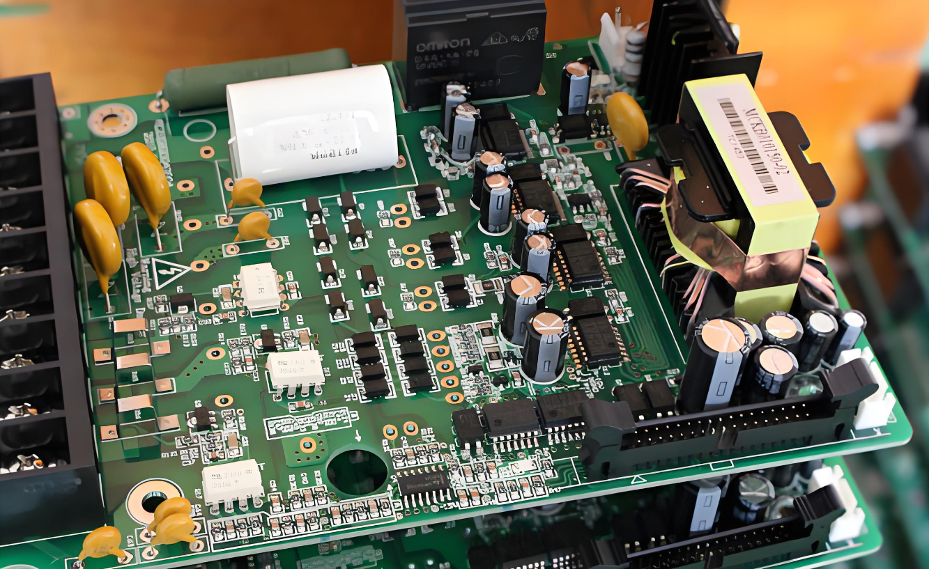
The plug-in processing process in PCB(printed circuit board) assembly is an important part of the electronic manufacturing process, which mainly deals with large-size components that cannot be automatically mounted by the machine due to size, weight or temperature tolerance. Plug-in processing process is roughly as follows:

First, preparation
Material preparation
Check BOM(Bill of Materials) : Ensure that the model, specifications, and quantity of all electronic components are consistent with the design requirements.
Component preprocessing: Pin processing of components that need plug-ins, adjust the pin spacing and Angle, and make it match the hole position of the PCB board. For some special components, it may be necessary to pre-cut the pin length for subsequent insertion.
PCB board inspection: Check whether the quality and specifications of the PCB board meet the requirements, including whether the board surface is flat and whether the hole position is accurate.
Tool preparation
Insert tools: Insert tools, such as pins, jigs, or tooling, for the accurate insertion of auxiliary components.
Welding tools: Prepare welding tools and materials such as welding table, solder, solder wire and flux.
Test devices: Test devices, such as multimeters and magnifying glasses, are ready for subsequent quality check.

Second, plug-in processing process
plug-in
Manual plug-in: For small-batch, complex or large-size components, manual plug-in is usually used. According to the PCB design document, the operator accurately inserts the components into the specified holes on the circuit board.
Automatic plug-in: For mass production, you can use an automatic plug-in machine for plug-in operation. Automatic inserters can quickly and accurately insert standard components such as resistors and capacitors.
Plug-in note:
Ensure that the surface of the components is clean and free from contaminants such as oil stains and paint, so as not to affect the welding quality.
The components and PCB board should be flat to avoid uneven welding.
If the component has a direction indication sign, the plug-in must be carried out in strict accordance with the direction indicated.
Insert moderate force to avoid damage to components or PCB board.
Crest welding
Preparation before welding: Before wave soldering, carefully check whether there is excess flux or other impurities on the PCB board, and thoroughly remove it.
Wave soldering process:
Put the PCB board into the conveyor belt of the wave soldering furnace.
After spraying flux, flux is used to remove oxides on welding surface and improve welding quality.
Enter the preheating zone to make the solder and welding surface reach the appropriate temperature.
Through the crest soldering tank, the molten solder crest electrically connects the pin of the cartridge component to the pad on the PCB board.
Finally, the solder joint is solidified through the cooling zone.
Welding parameter setting: According to the component type and circuit board material, adjust the temperature of the wave welding furnace, conveyor speed, wave peak height and other parameters to ensure the welding quality.
Shear pin
Pin operation: Because the pins of the DIP(Dual in-line package) components extend beyond the PCB surface, pin treatment is required to achieve the appropriate size.
Precautions for cutting feet: Be careful when cutting feet to avoid damage to welding joints. Special foot cutting tools or equipment can be used for foot cutting operations.
Post welding
Objective: To repair the welding defects that may occur in the welding process, such as continuous tin, less tin, lack of tin, etc.
Operation: Use manual welding tools such as electric soldering iron to repair welding of incomplete or poorly welded components.
cleanse
Objective: To remove the residual flux and other contaminants in the welding process, and ensure that the PCB surface is clean.
Cleaning method: chemical cleaning, ultrasonic cleaning and other methods can be used. After cleaning, use a clean cloth or paper towel to dry the PCB surface.

Third, quality inspection and testing
Visual inspection
Check content: Check solder joint quality, component installation position, PCB board for damage, etc. The solder joint should be full, smooth, free of defects such as virtual welding and short circuit.
Inspection tools: Magnifying glass, microscope and other tools can be used to assist the inspection.
Functional testing
Test purpose: To verify the function of PCBA(printed circuit board assembly).
Test method: Use professional equipment for functional testing of PCBA finished boards, such as online testing (ICT), functional testing (FT), etc. The test includes electrical properties such as circuit connectivity and resistance values, as well as functional tests in simulated real working environments.
Fourth, finished product packaging and delivery
package
Esd packaging: ESD packaging materials, such as ESD bags and foam, should be used for electrostatic sensitive electronic components.
Mark and record: mark the product name, specification, quantity, production date and other information on the package, and attach the inspection report and certificate of conformity.
Deliver goods
Pre-shipment inspection: Before shipment, the packaged products are checked again to ensure that the quantity is correct and the packaging is intact.
Logistics arrangements: Choose the right logistics methods to ensure that products can be safely and on time to the hands of customers.
Through the above plug-in processing process, it can ensure the accurate installation and reliable connection of large-size components on the PCB board, providing a strong guarantee for the normal operation of electronic products. In actual operation, the process specifications and quality standards should be strictly observed to ensure that every step of the operation is to achieve the best results.


