- Home
- Products
- Industrial Control PCB Assembly
- Communication equipment PCB Assembly
- Automotive Electronics PCB Assembly
- Medical Device PCB Assembly
- Security Electronics PCB Assembly
- Consumer Electronics PCB Assembly
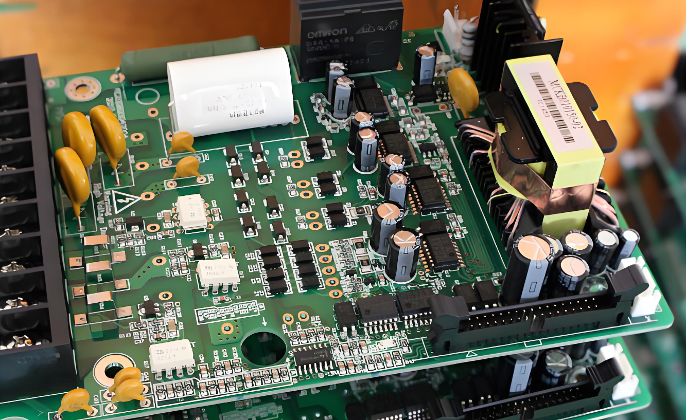
- Power Electrical PCB Assembly
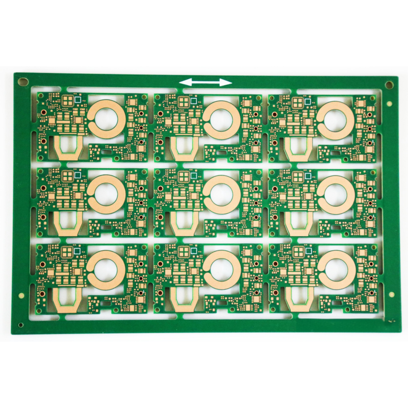
- Double-Sided PCB Manufacturing
- Multilayer PCB Manufacturing
- HDI PCB Manufacturing
- Rigid-Flex PCB Manufacturing
- OEM Product PCBA Solutions
- About Us
- OEM/ODM
- Solutions
- Service
- Blogs
- Contact Us
Please Choose Your Language
- English
- العربية
- Français
- Русский
- Español
- Português
- Deutsch
- italiano
- 日本語
- 한국어
- Nederlands
- Tiếng Việt
- ไทย
- Polski
- Türkçe
- አማርኛ
- ພາສາລາວ
- ភាសាខ្មែរ
- Bahasa Melayu
- ဗမာစာ
- தமிழ்
- Filipino
- Bahasa Indonesia
- magyar
- Română
- Čeština
- Монгол
- қазақ
- Српски
- हिन्दी
- فارسی
- Kiswahili
- Slovenčina
- Slovenščina
- Norsk
- Svenska
- українська
- Ελληνικά
- Suomi
- Հայերեն
- עברית
- Latine
- Dansk
- اردو
- Shqip
- বাংলা
- Hrvatski
- Afrikaans
- Gaeilge
- Eesti keel
- latviešu